3.1. Microstructure
The porous microstructure of graphite consists of cracks, open and closed pores, and grain boundaries at a macroscopic scale.
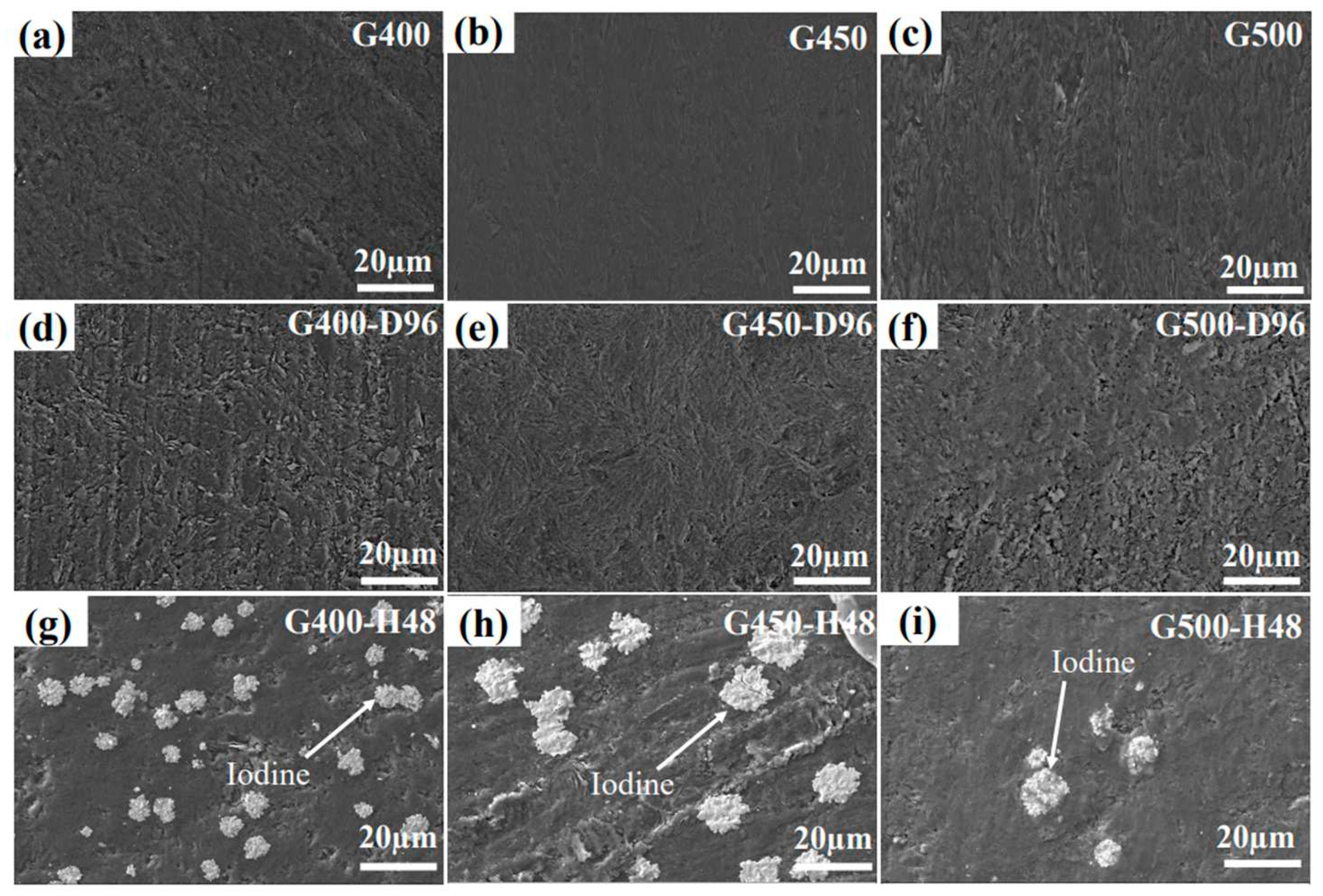
Figure 2(a-c) show the surface structure of micro/nano-porous graphite before iodine diffusion. Nanoporous graphite G400 and G450 have a smoother surface structure than microporous graphite G500, while the surface structure of G450 is more perfect than that of G400.
Figure 2(d–f) shows the SEM images of graphite surfaces of G400, G450, and G500 diffused in iodine vapor at 650°C for 96 h. Compared with the microscopic morphology of the graphite surface in the original state, the surface of the diffused graphite becomes rougher. But the surface texture of G450 graphite is not as clear as that of G400 and G500, because G450 graphite is least affected by iodine vapor (G450 has the smallest average pore size).
Figure 2(g–i) shows iodine-loaded micro/nano-porous graphite undergoing isothermal annealing for 48 h at the same temperature and vacuum to observe the diffusion of iodine from the inside of the graphite to the surface. Interestingly, iodine was precipitated near the pores on the surface of graphite after the annealed graphite stood at room temperature for a period of time, which indicates that pores are an important channel for graphite diffusion.
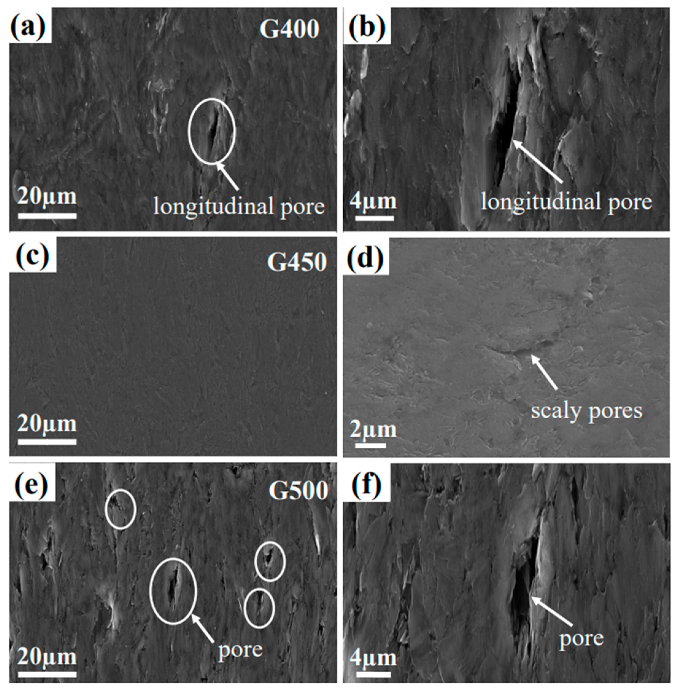
Random cracks and pores could be identified in the micro/nano-porous graphite of the pristine structure as shown in
Figure 3.
Figure 3a and 3b show large longitudinal pores inside G400, which are generated by the interaction between volatile gas escape during graphitization and anisotropic contraction of graphite crystals during the cooling phase of graphite manufacturing. Compared with G400 and G500, nanoporous graphite G450 has a smooth surface and small pore size. However, G450's surface occasionally has scaly transverse pores. The pores on the surface of G500 are large and uniform, and these pores are caused by volatiles in the adhesive during the sintering process.
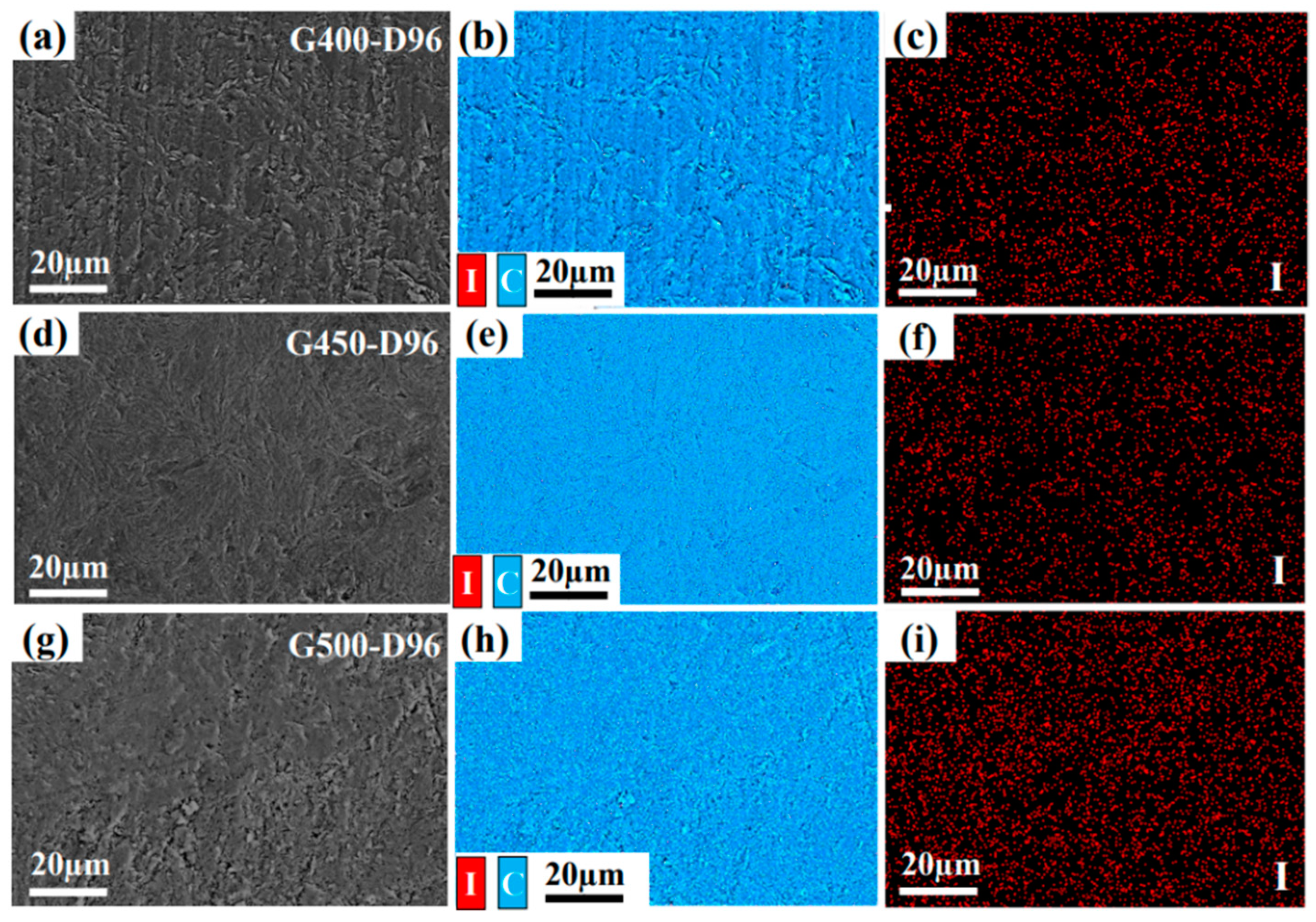
Figure 4 shows the EDS image of G400, G450 and G500 graphite diffused in iodine vapor for 96 h at 650 °C, respectively. The distribution of iodine diffusion is on the graphite surface, and the blues and reds in
Figure 3 (b-c, e-f, and h-i) represent carbon and iodine, respectively. The relative content of iodine in G400, G450 and G500 are the same as that of energy dispersive spectrometer (EDS) analysis, as shown in
Table 3. Since the diffusion of gaseous substances generally includes two processes of adsorption and diffusion, the smooth graphite surface is not easy to adsorb and diffuse substances. Iodine vapor is not easily attached to the smooth G450 graphite surface, so the iodine content on the surface of G450 is smaller than that of G400 and G500.
3.2. Rutherford backscattering spectrometry analysis
Rutherford backscattering spectrometry (RBS) is an efficient analytical method for detecting the diffusion depth of elements with higher atomic numbers in the periodic table in a matrix material for elements with lower atomic numbers [
15,
16].
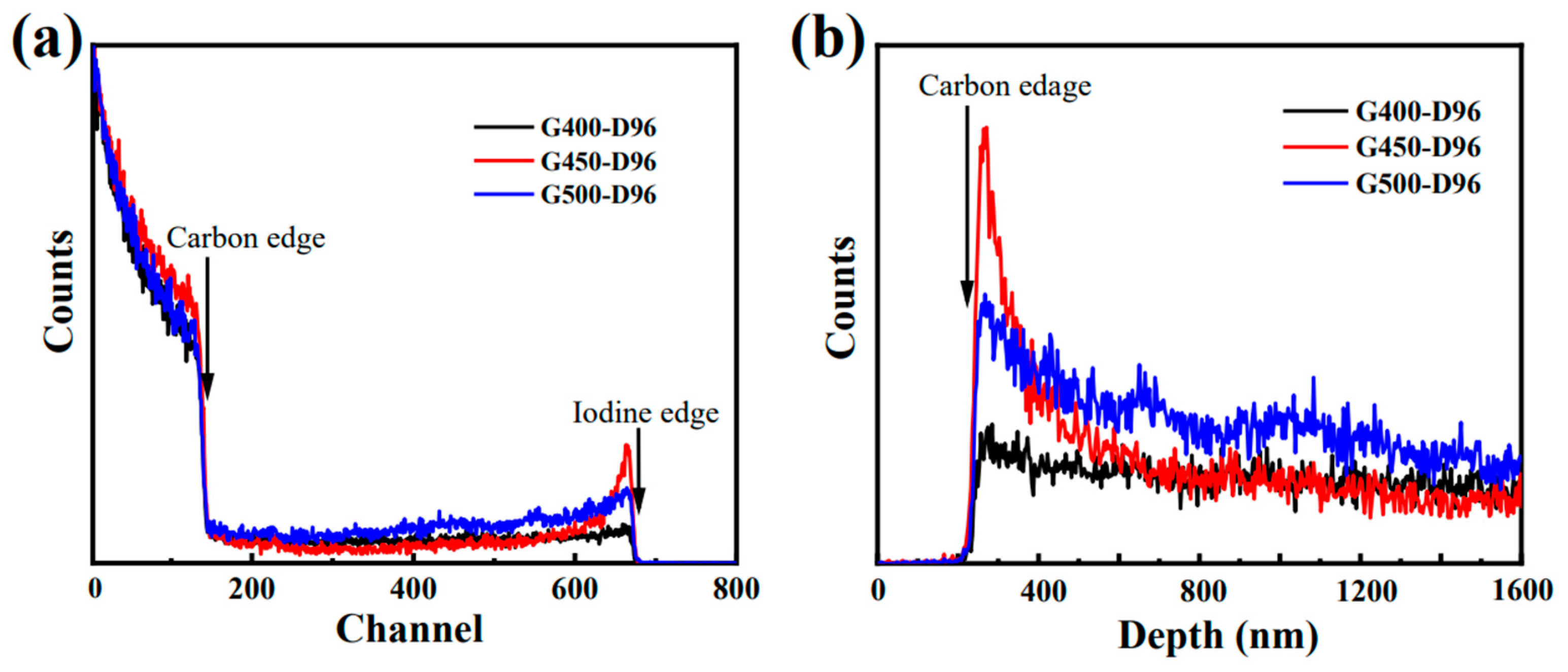
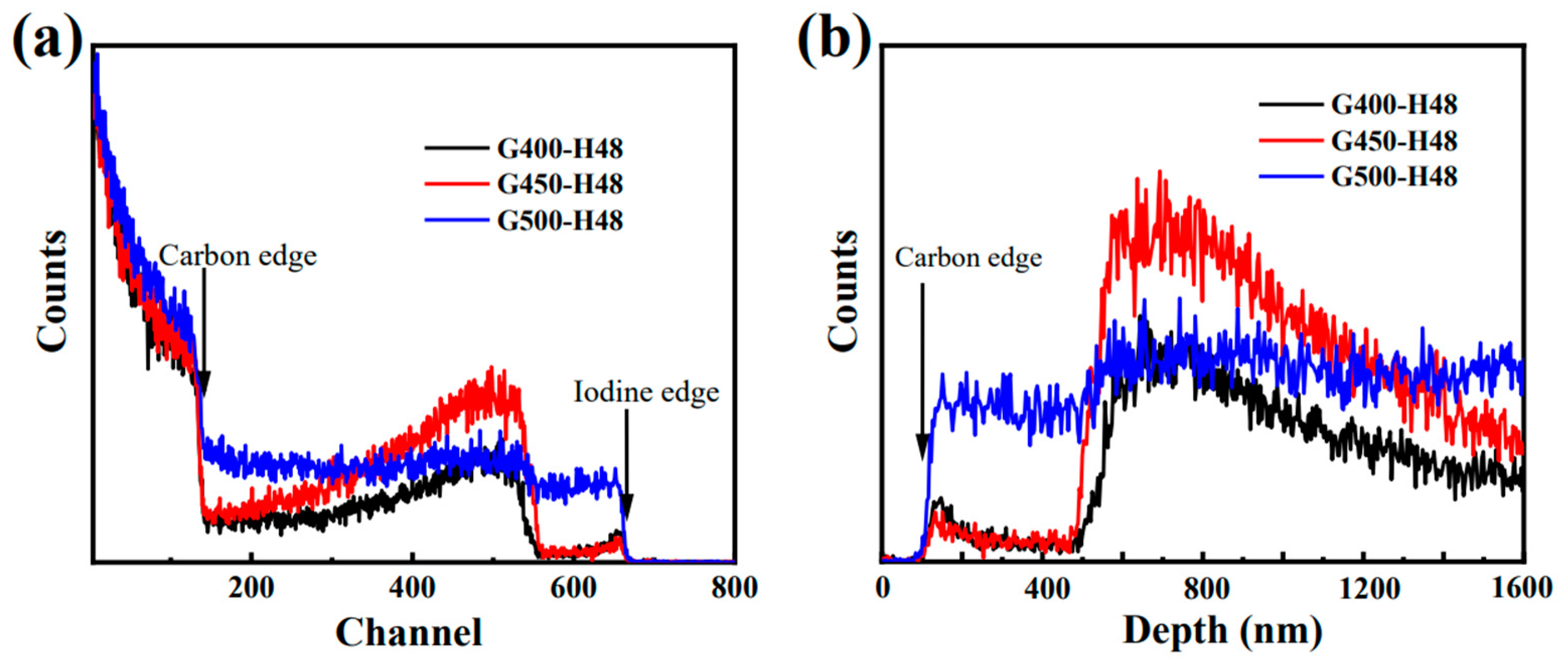
Figure 5a shows the RBS experimental spectra of micro/nano-porous graphite (G400, G450, and G500) after diffusion in iodine vapor at 650 °C for 96 h. The respective surface channel positions of C and I are indicated by arrows, and the distribution of I presents a distribution in which the concentration gradually decreases from the surface to the interior.
Figure 5b shows the depth profiles of micro/nano-porous graphite (G400, G450, and G500) after diffusion in iodine vapor at 650 °C for 96 h. The difference in iodine distribution between nanoporous graphite G400 and G450 and microporous graphite G500 is shown in
Figure 5a and 5b. The RBS experimental spectrum shows that after diffusing in iodine vapor at 650 °C for 96 h, the iodine content of G450 and G500 gradually decreases from the graphite surface to the interior of the matrix, while the iodine content of G400 has little difference between the surface and interior of graphite. The iodine content on the surface of G450 is higher than that of G400 and G500, which seems to be contradicted by the EDS analysis results that the iodine content on the surface of G450 is the least. The implementation is just the opposite, since the diffusion of gaseous species is related to the pore size and cracks of graphite. Nanoporous graphite G450 has a smaller average pore size, less defects such as cracks, and its surface is smooth. Although G400 graphite is also nanoporous graphite (average pore size is 23nm), its surface has cracks and large longitudinal pores. These larger cracks and longitudinal pores make the connected pore network on the surface of G400 larger (17.8% open porosity), resulting in little difference between its surface and internal iodine. These data results indicate that larger cracks and longitudinal pores propagate more easily. Both G450 and G500 graphite have a common point that the pore distribution is relatively uniform. The difference is that the open porosity of G450 (17.3%) is higher than that of G500 (12.8%),while the average pore diameter of G500 (553nm) is bigger than that of G450 (18nm). It can be seen from
Figure 5a and 5b that there is more iodine on the surface of nanoporous graphite G450 with a depth of less than 400nm than that of G500, because the graphite surface with a larger open porosity is more likely to capture iodine. But at depths greater than 400 nm, the iodine distribution of both nanoporous graphite G400 and G450 are lower than that of microporous graphite G500. The iodine distribution of G450 graphite is the smallest of the three graphite, which is caused by its smaller average pore size and fewer frontal defects. In short, nanoporous graphite G450 has better performance of blocking iodine diffusion in the process of adsorption and diffusion.
Figure 6a shows the experimental RBS spectra of iodine-loaded micro/nano-porous graphite (G400, G450 and G500) annealed for 48 h under vacuum at 650 °C to describe the desorption and diffusion behavior of iodine-loaded graphite.
Figure 6b shows the depth distribution of iodine, and the surface of C is marked with arrows. Annealing causes iodine to diffuse deeper into the graphite. Since part of the iodine on the graphite surface is rapidly released during annealing, and the internal iodine continues to diffuse to the surface, a wide iodine peak appears in all three graphites at 650nm from the graphite surface. However, the iodine peak of microporous graphite G500 at 650 nm is not pronounced due to the formation of a stable iodine diffusion channel inside the G500 of the larger pore [
17,
18]. At depths greater than 1.4 µm, nanoporous graphite G400 and G450 have less iodine than microporous graphite G500, indicating that pore size is a key factor affecting iodine diffusion performance, and nanoporous graphite has better performance in blocking iodine diffusion than microporous graphite. Combined with the results of SEM surface morphology analysis, the nanoporous graphite G450 has the best performance in blocking iodine diffusion owing to smaller pores, fewer cracks and smoother surface.
3.3. Crystal structure
In order to illustrate the effect of iodine diffusion on graphite microstructure, the diffraction angle of (002) peak and Bragg formula were used to analyze the variation of graphite interlayer spacing. According to the Bragg formula 2dsinθ=nλ and d
c=(d-d
1)/d (where d
c is the change in interlayer spacing, d is the interlayer spacing of the original graphite, and d
1 is the graphite interlayer spacing after iodine diffusion) to calculate the graphite interlayer spacing before and after diffusion amount of change.
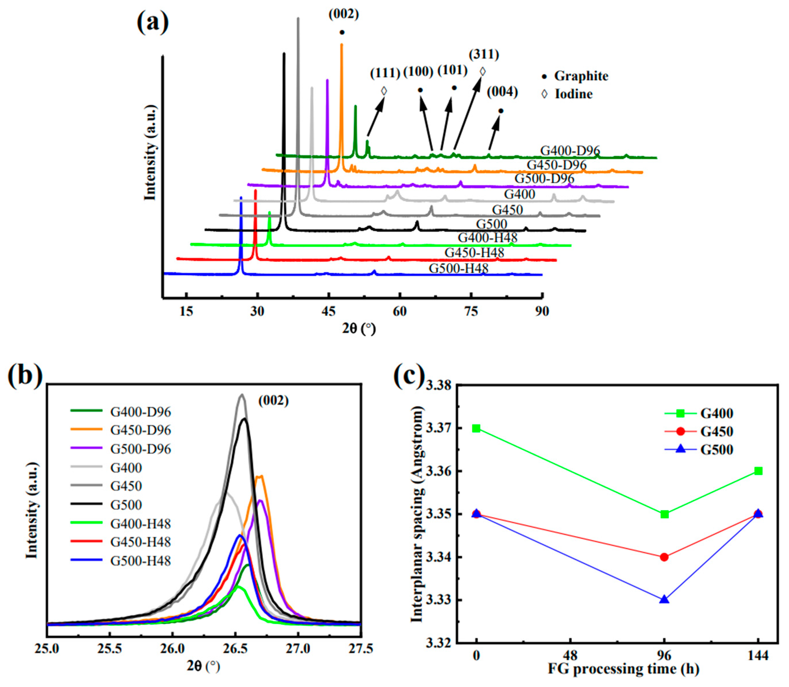
Figure 7(a-c) show the X-ray diffraction (XRD) patterns of micro/nano-porous graphite (G400, G450 and G500) of different experimental conditions, including the change trend of micro/nano-porous graphite (002) peak, and the change trend of micro/nano-porous graphite interlayer spacing under different treatment time, respectively.
Figure 7a shows that the (111) peak near the (002) peak indicated the iodine diffuses into micro/nano-porous graphite at 650°C, which is similar to the peaks that appear near the (002) peak of graphite in the literature due to the presence of silicon impurities [
19,
20].
Figure 7(a-b) shows the XRD spectra of microporous graphite, adsorption diffusion and isothermal annealing processes in the original state, and the presence of (111) peaks is thought to be related to iodine diffusion.
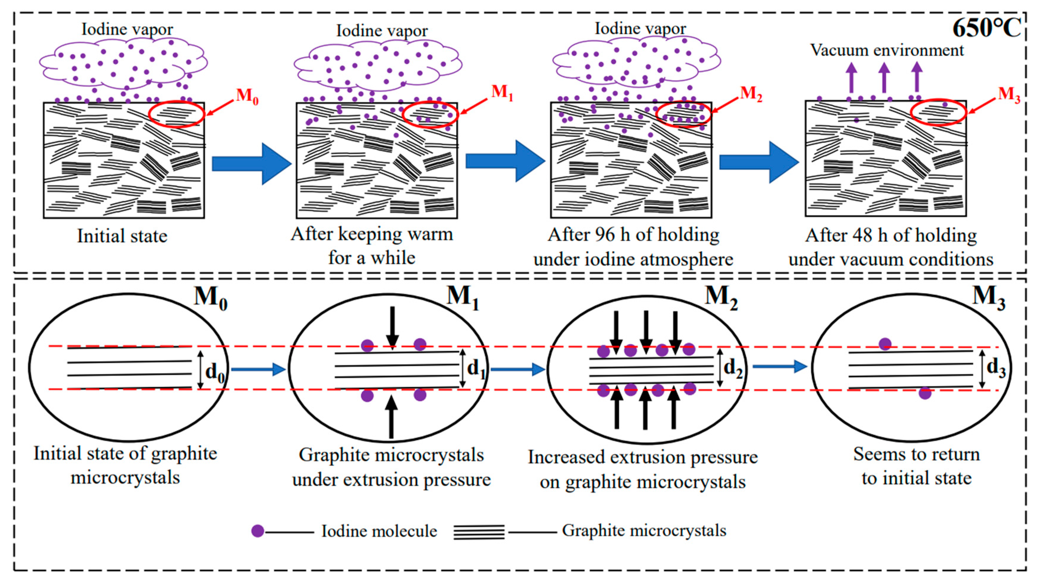
Figure 7c shows graphite layer spacing vs. iodine diffusion. With the diffusion of iodine into graphite, the interlayer spacing of graphite decreases, while after iodine diffuses from graphite, the interlayer spacing of graphite tends to recover. This recoverable process is more like a physical reversible process. The decrease in the spacing of graphite layers is considered to be the internal stress caused by the diffusion of iodine and the mutual extrusion between graphite layers. However, the mechanism of their internal stress interaction needs further study. The abscissa of 144 h in
Figure 7c is derived from the addition of two times, including the graphite sample first subjected to a 96-h iodine diffusion experiment and 48-h vacuum annealing experiment. The diffraction angle of d
002 increased by 2θ due to iodine diffusion into graphite samples. But when iodine diffuses out during annealing, d
002 seems to return to its initial state, which may be that iodine diffusion into the graphite grain boundary causes the graphite crystal to shrink along the c-axis. However, the shrinkage caused by diffusion is small (as iodine diffuses into graphite, the interlaminar spacing of nanoporous graphite G400 and G450 decreases by 5.9‰ and 2.9‰, respectively, and the interlaminar spacing of microporous graphite G500 decreases by 6.0‰) and can be restored. During the vacuum isothermal annealing process, the iodine on the graphite surface diffuses out, and the interlayer spacing of graphite returns to its original state because it is no longer squeezed. These data indicate that iodine diffuses at high temperature with little energy and the effect on graphite crystals is recoverable [
13]. The smaller the change in the spacing of graphite layers, the less affected the graphite structure is affected by iodine diffusion. The layer spacing change of nanoporous graphite is smaller than that of microporous graphite, which can effectively prevent the diffusion of iodine. The spacing change of the nanoporous graphite G450 layer was the smallest (2.9‰) by comparing the spacing changes of the three graphite layers. Nanoporous graphite G450 has the best effect of blocking iodine diffusion, which is consistent with the results of previous analyses.
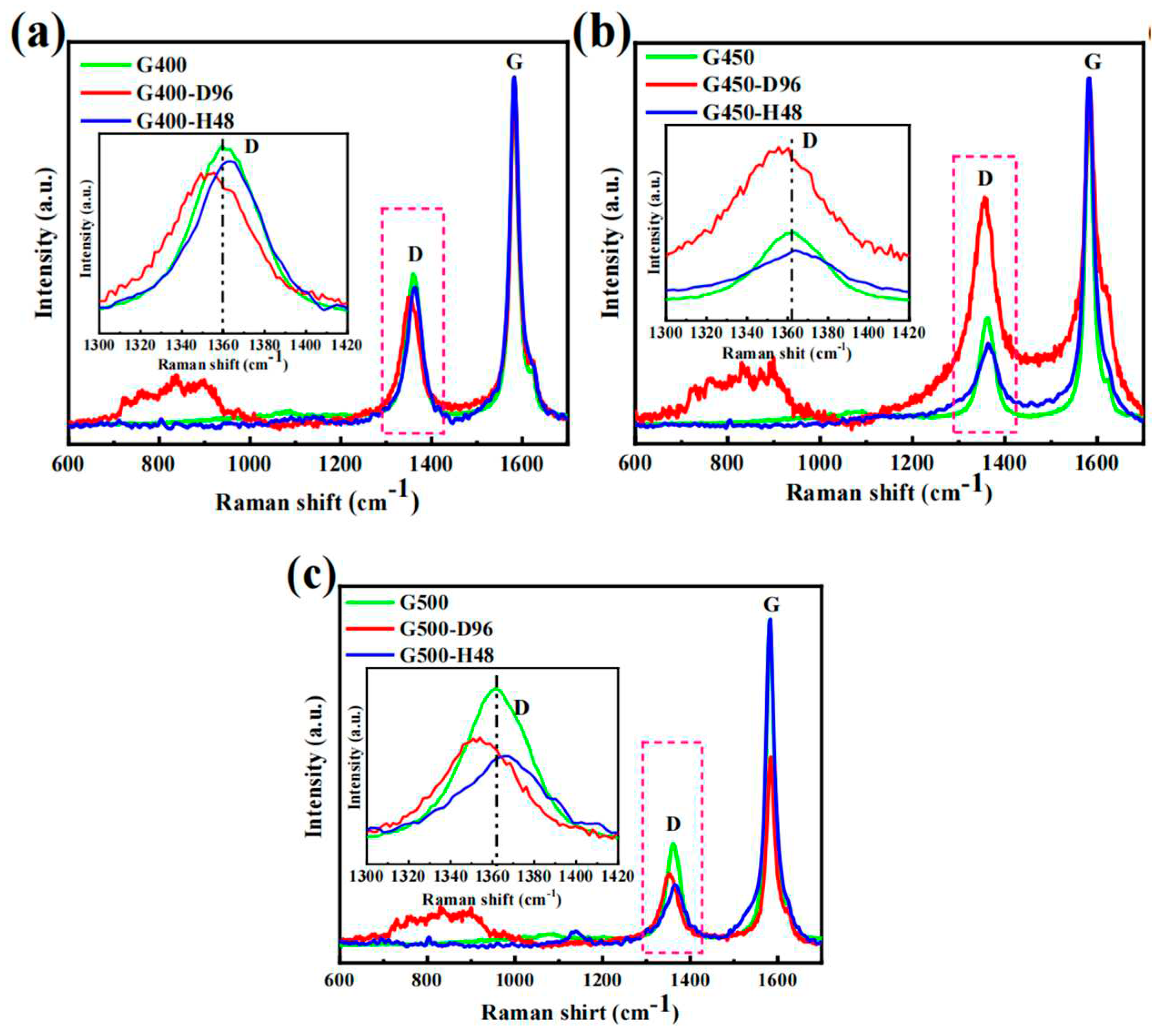
Raman spectra of micro-nanoore graphite samples before and after the diffusion experiments were analyzed at a laser wavelength of 473 nm and an effective penetration depth of about 50 nm. The typical D and G characteristic bands of graphite were detected in the Raman band of 1300 cm
-1 to 1700 cm
-1 [
14]. The position of the D peak signal in the Raman spectrum is independent of the defect type, and its appearance only requires the defect to participate in the phonon dispersion process to meet the momentum conservation law [
15]. The pristine G400, G450 and G500 of the D and G peaks of the Raman spectra appear at about 1361 cm
-1 and 1582 cm
-1, respectively. The D band strength I
D of graphite depends on the defect type and density. The strength ratio (I
D / I
G) of D band and G band are used to evaluate the grain size and graphitization degree [
16]. Based on the integral area ratio between the D peak and G peak intensities, called I
D and I
G, respectively. The following equation was used to calculate the microcrystal size L
a [
17]:
.
As shown in
Table 4, the microcrystalline size L
a of micro/nano-porous graphite (G400, G450 and G500) decreases with iodine diffusion into this graphite. While L
a increases when iodine diffuses out of graphite (annealing process of iodine-loaded graphite). The decrease in the L
a value indicates that the graphite crystallites are subjected to extrusion forces in the a-axis, which is consistent with the result that the diffusion of iodine causes the graphite crystals to shrink along the c-axis by XRD patterns (
Figure 7c). However, L
a is larger after annealing simply because the graphite microcrystals grow further after iodine diffusion out of the graphite. Usually, the relative intensity ratio of I
D/I
G is used to characterize the defect density of graphite [
18]. The increase in I
D/I
G of micro/nano-porous graphite (G400, G450 and G500) after iodine diffusion is caused by the increase in defect density in graphite due to iodine diffusion. After annealing, the iodine escapes from the graphite matrix and the I
D/I
G of graphite decreases, indicating a decrease in defect density.
Figure 8 shows that after 96 h of iodine diffusion at 650 °C, the position of D peak shifts to the left. The iodine diffused into the pores causes internal stress between the graphite flakes of graphite, which elastically deforms the graphite microcrystals. After annealing, the iodine diffuses out of the graphite matrix, and the position of the D peak is recovered due to the extrusion force of graphite microcrystals is weakened. These phenomena suggest that iodine diffusion affects the elastic or inelastic scattering of phonons, causing the movement of the D peak. The stocky Raman band between 500 cm
-1 and 1300 cm
-1 is considered a Raman characteristic peak of iodine vapor because this stocky peak disappears after annealing [27–29]. These data shown that the diffusion process of iodine only causes the deformation of graphite microcrystals without destroying the structure of graphite.
Table 4.
Raman shifts of D and G peaks of graphite and the ratio of the intensity ID/IG.
Table 4.
Raman shifts of D and G peaks of graphite and the ratio of the intensity ID/IG.
| Sample name |
D peak wave
number (cm-1) |
G peak wave
number (cm-1) |
ID/IG
(arbitrary units) |
La (nm) |
| G400 |
1361 |
1583 |
0.34 |
35 |
| G400-D96 |
1353 |
1582 |
0.39 |
31 |
| G400-H48 |
1362 |
1582 |
0.28 |
43 |
| G450 |
1362 |
1583 |
0.32 |
38 |
| G450-D96 |
1356 |
1583 |
0.63 |
19 |
| G450-H48 |
1362 |
1582 |
0.23 |
52 |
| G500 |
1361 |
1581 |
0.32 |
38 |
| G500-D96 |
1354 |
1583 |
0.38 |
32 |
| G500-H48 |
1365 |
1583 |
0.20 |
60 |
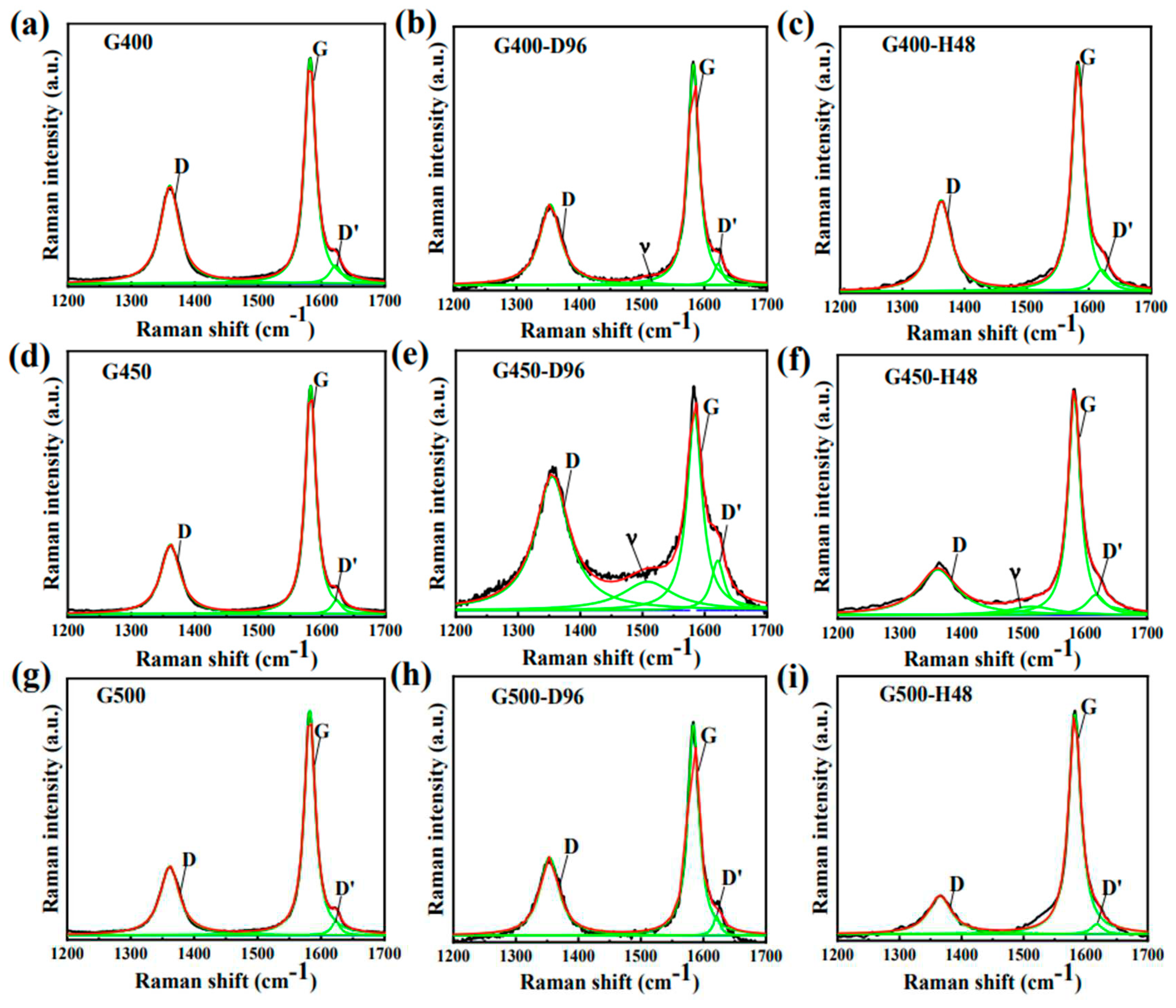
Figure 9 shows the Raman spectra yields of the D peak, D' peak and G peak. The D Peak (1361 cm
-1) is caused by the elastic scattering caused by the defect at the crystal boundary inside the graphite [
22]. With the diffusion of iodine into and out of the graphite, the peak intensity (I
D') of D' peak increased first and then decreased. The D' peak (1622 cm
-1) is relevant to the elastic scattering of vacancy defects near graphene [
23]. The diffusion of iodine into the graphite led to the increase of the defect density. After the iodine diffuses into fine-grained graphite, the Raman curves show v peak (
Figure 6a
1 and 6b
1). As the Ferrari's stated, the presence of the v peak is due to trans-polyacetylene in the grain boundary [30,32]. The phenomenon of v peak after iodine diffusion due to the diffusion of iodine into the graphite grain boundary, which affects the trans-polyacetylene in the grain boundary. It is further explained that the changes caused by iodine diffusion for fine-grained graphite are physical processes and also reversible processes. And this is consistent with the previous discussion.

