
Submitted:
06 July 2023
Posted:
11 July 2023
You are already at the latest version
Abstract
In order to improve the charge collection efficiency, we simulated and experimentally tested the doping structure of the electron multiplication layer in EBCMOS. In this paper, we simulate the charge collection efficiency of EBCMOS under different doping methods by modeling the collisional scattering of electrons with solid atoms in semiconductor materials and combining the transport trajectories of electrons in the electron multiplication layer, the simulation results indicate that using a layered doping structure to reduce the thickness of the index heavily doped layer can effectively optimize the electric field distribution in the electron multiplier layer and reduce the recombination rate of electrons. The optimized doping structure has a significant effect on improving charge collection efficiency. Based on the simulation results, doped samples were prepared and tested. The test results showed that the charge collection efficiency obtained under the condition of a P-type silicon substrate thickness of 7μm and an index heavily doped layer thickness of 1μm was 72.65%, reducing the thickness of the index heavily doped layer to 0.1μm, the charge collection efficiency obtained can reach 86.27%, which proves that reducing the thickness of the index heavily doped layer can effectively improve the charge collection efficiency of EBCMOS devices.
Keywords:
EBCMOS
; Monte Carlo
; electric field distribution
; charge collection efficiency
1. Introduction
In the early reported EBCMOS devices, the electron multiplication layer structure in EBCMOS devices is mostly uniformly doped, and the charge collection efficiency obtained by this doping method is low due to the inability to generate an internal electric field in the multiplier layer that is conducive to electron transport, and the extremely low electron lifetime under uniform heavily doped conditions. In the later research on EBCMOS, gradient doping was applied to the electron multiplier layer to generate an internal electric field in the multiplier layer, resulting in a significant improvement in charge collection efficiency[1]. In the process of studying exponential doping on P-type silicon substrate to improve charge collection efficiency, we found that layered exponential doping on P-type silicon substrate can improve the obtained charge collection efficiency, and thinning the heavy exponential doping structure in layered exponential doping structure can further improve the obtained charge collection efficiency. In the experimental part, P-type silicon substrate with substrate doping concentration of 1014atom/cm3 was selected. TRIM software was used to perform ion implantation simulation on P-type silicon substrate, and ion implantation was performed on P-type silicon substrate according to the simulation results, the test results show that under the condition of input current of 25nA and acceleration voltage of 8kV, the measured output current of the sample after thinning the dopant layer is 1.69μA, and the calculated charge collection efficiency is 87.32%, while that of the sample without thinning is 73.5%. It is proved that the electron collection efficiency can be effectively improved by reducing the thickness of the heavily doped layer when the P-type silicon substrate is layered with exponential doping.
2. Materials and Methods
EBCMOS devices thin the back substrate of front-facing CMOS devices, and use the back of the sensor as the anode. Photoelectrons generated by the photocathode after light excitation are accelerated and bombarded to the back of the sensor under the action of space electric field, high-energy electrons are generated by colliding with solid in the electron multiplication layer of EBCMOS, thus obtaining bombardment semiconductor gain[2]. The multiplier electrons are eventually collected in the collection area N-well to read out the electrical signal. The electron gain multiple G obtained in the electron multiplier layer can be expressed by , where ε is the collection efficiency of electrons, is the initial energy of electrons, is the energy lost by electrons passing through the passivation layer, and 3.6 is the energy loss required to produce an electron-hole pair. With constant and , increasing the charge collection efficiency ε can effectively improve the electron gain in the multiplier layer. In order to improve the efficiency of charge collection, factors such as the lifetime of secondary electrons in the electron multiplier layer, the accelerated transport of electrons by electric field in the multiplier layer and the collision scattering of electrons should be considered.
2.1. Physical model of electron collision scattering process
The electron beam is accelerated by the close focusing structure and bombarded to the surface of the passivation layer, passing through the passivation layer and entering the multiplication layer. In the multiplier layer, electrons collide with solid atoms in the P-type silicon substrate, and secondary electrons are generated in the collision process to obtain the bombarding semiconductor gain. The collision scattering process can be divided into elastic scattering and inelastic scattering according to whether the energy is lost. In the elastic scattering process, the direction of electron movement changes, and the energy loss is very low and can be ignored. In the process of inelastic scattering, the collision of electrons with solid atoms will not only change the direction of motion, but also lose energy, in which the lost energy will be manifested in the form of secondary electrons, and the process of energy loss can be calculated by the Bethe incapacity formula. In practice, the voltage of the close focusing structure in the EBCMOS is generally less than 30kV, so the scattering cross section between the electron and the solid atom can be calculated using the modified Rutherford elastic scattering cross section formula for low energy electrons [3]:
The energy loss process of electrons also selects the modified Bethe incapacitation formula applicable to low-energy electrons:
Then the spatial position change of electrons after a single scattering process can be calculated as follows:
In the above formula, for single scattered step length, the scattering azimuth Angle , scattering Angle , =3.4×10³, is the Rutherford elastic scattering shielding coefficient, are random numbers in (0,1).
2.2. Physical model of electron trajectories
The electron multiplication process can be regarded as the injection of non-equilibrium carriers. In the electron multiplication layer, the electron concentration on the side near the dead layer is much higher than that on the side near the collection zone. In this case, the electrons will diffuse from the dead layer side to the collection zone under the action of concentration gradient. Assuming that the number of incident photoelectrons is the same in each integral time, the diffusion motion of electrons in the multiplier layer can be regarded as the injection of steady-state non-equilibrium carriers, and the diffusion velocity of electrons can be expressed as follows [4]:
In the case of uniform doping, no built-in electric field is generated in the multiplier layer, and electrons are only transported to the depletion region by diffusion, resulting in low charge collection efficiency. Therefore, it is necessary to perform exponential doping on the multiplier layer, which can obtain the built-in electric field conducive to the transport of electrons in the multiplier region. Assuming exponential doping is adopted for the multiplication region, the doping impurity concentration is calculated as , where represents the impurity doping concentration at depth z, is the doping concentration at depth 0, and is the calculation parameter determined by the depth and doping concentration in the doping region. In this case, an internal electric field will appear in the doping region. The field strength of the built-in electric field satisfies the following formula[5]:
Where is the Boltzmann constant, is the temperature, and is the charge of the electron, it can be seen that increasing can effectively improve the strength of the built-in electric field. The electron migration speed under the combined action of the built-in electric field and the concentration gradient can be expressed as follows:
Where V is the drift velocity of the electron under the action of the built-in electric field, which can be expressed by the formula , is the component of the velocity of the electron under the action of the built-in electric field in the direction of Z axis.
2.3. Effect of doping structure on minority carrier lifetime
In P-type silicon, the minority carrier lifetime is negatively correlated with the concentration of doping impurities, and the minority carrier lifetime can be expressed by the following empirical formula, where is the concentration of doping impurities:
Set the doping approach to uniform doping, doped impurity concentration of boron atoms were set up to 1019atoms/cm3, 1015atoms/cm3 and 1014atoms/cm3, In this case, the minority carrier lifetimes are 2.2727×10⁻⁸s, 2.8985×10⁻⁴s and 2.9×10⁻³s. The doping mode is set as overall exponential doping, and the impurity concentration varies with depth as . When z=7, = 1014atoms/cm3, and the life curve of minority carriers with depth is shown in Figure 1:
It is found that the electron lifetime is lower than 1×10⁻⁴s at the depth of 0~5μm, and the charge collection efficiency is mainly limited by the electron lifetime. In order to reduce the electron recombination rate, it is necessary to try to thin the heavy exponential doping layer. The doping mode is set as layered exponential doping, the concentrations at both ends of the heavy exponential doping layer are 1019atoms/cm3 and 1015atoms/cm3 respectively, and two thicknesses of the heavy exponential doping layer are set, the thicknesses of the heavy exponential doping layer are 1μm and 0.1μm respectively. At this time, the life curve of a few carriers in the heavy exponential doping layer with depth is shown in Figure 2:
By analyzing the minority carrier lifetime in the reduced heavy exponential doping structure, it is found that in the 0.1μm thick heavy exponential doping structure, the minority carrier lifetime is less than 1×10⁻⁴s only in the depth of 0~0.09μm, in the 1μm thick heavy exponential doping layer, the minority carrier lifetime of electrons is lower than 1×10⁻⁴s in the depth of 0~0.9μm. Therefore, thinning the heavy exponential doping layer can be considered to improve the charge collection efficiency.
2.4. Effect of thinning heavy exponential doped layer on electron drift velocity
In semiconductors, the drift speed of electrons is determined by electron mobility and electric field strength, electron mobility can be calculated by Matthieseen's law:
In the above formula, is the acoustic phonon scattering mobility, is the ionized impurity scattering mobility, is determined by the type of semiconductor, and is negatively correlated with the impurity doping concentration. The electron migration rate in the semiconductor can be calculated by the following formula:
Because the impurity concentration at the end of the heavy exponential doping layer is still 1015atoms/cm3 after thinning, the electron mobility at the end of the heavy exponential doping layer remains unchanged, and the impurity concentration in the heavy exponential doping layer is , when the thickness of heavy index doping layer is 1μm and 0.1μm respectively, =9.2, =92, according to Equation 5, thinning the thickness of the heavy exponential doping layer can greatly improve the strength of the built-in electric field, increase the speed of electrons passing through the low minority carrier lifetime region, and reduce the time of electrons passing through the low minority carrier lifetime region. Therefore, thinning the thickness of the heavy exponential doping layer is conducive to improving the charge collection efficiency.
3. Simulation of charge collection efficiency under different doping structures
3.1. Charge collection efficiency under uniform doping
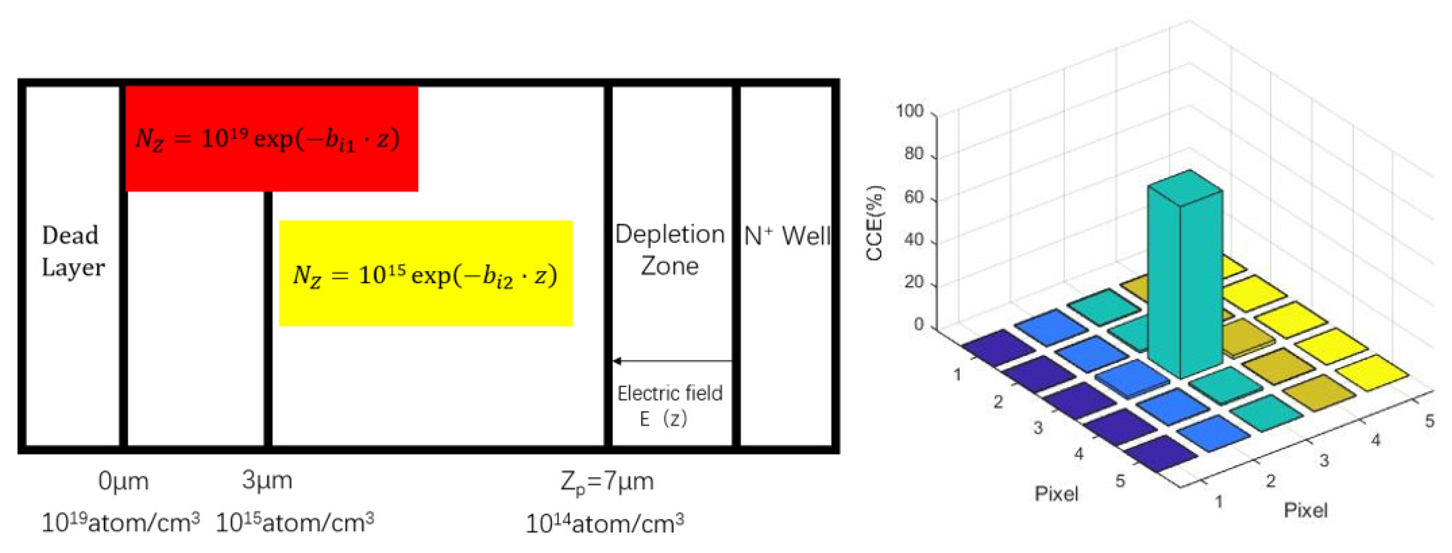
The doping structure is set as uniform doping, the incident electron energy is 4KeV, the electron beam diameter is 20nm, the dead layer thickness is 60nm, the P-epitaxial layer thickness is 10μm, the doping impurity is boron atoms, and the doping concentration is set to 1019atoms/cm3. After simulation, the charge collection efficiency in the 5×5 pixel region is 6.06%, as shown in Figure 3:
It can be seen that the charge collection efficiency of the uniform heavily doped structure is low, which is due to the decrease of the lifetime of the minority carriers in the doubling layer caused by the high doping concentration. At the same time, the electric field conducive to electron transport is not established in the doping region, so the electrons cannot be effectively transported to the N-well. Next, exponential doping is used to generate a built-in electric field that accelerates electron drift in the multiplier region.
3.2. Charge collection efficiency under overall exponential doping
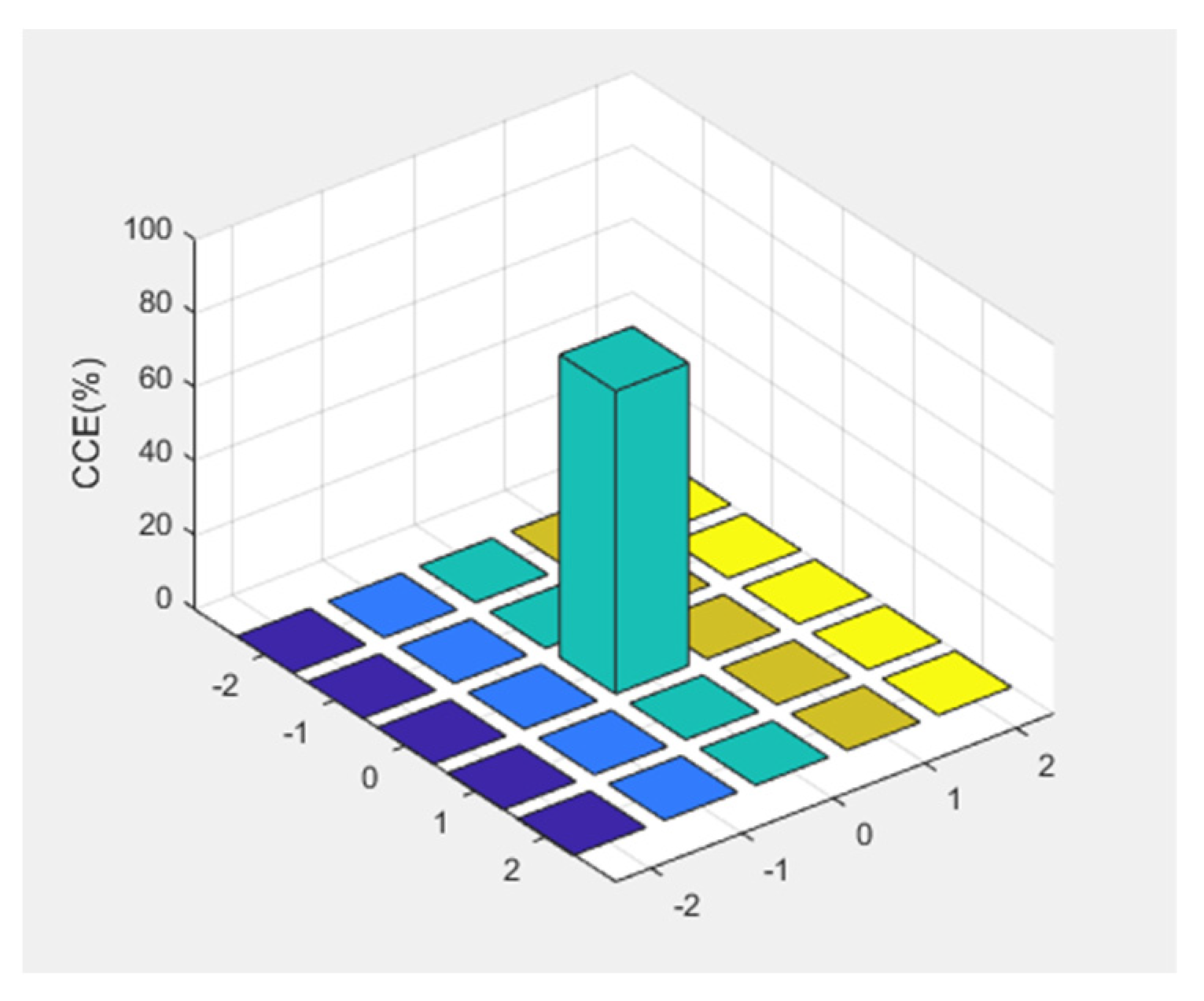
The impurity concentration in the multiplier layer is set as exponential distribution. When 0 < z < 7, the overall exponential doping is carried out with , , the incident electron energy is 4KeV, the electron beam diameter is 20nm, and the dead layer thickness is 60nm. The thickness of P-type silicon epitaxial layer is 10μm, and the charge collection efficiency in the obtained 5×5 pixel region is 54.74%, as shown in Figure 4:
At this time, the charge collection efficiency obtained is still at a low level, although there is an internal electric field in the doping region. The factors affecting the charge collection efficiency are analyzed, and the reason is that the electric field intensity of the internal electric field in the exponential doping region is low at this time, and the non-equilibrium carrier lifetime is also low, leading to a high recombination rate. Therefore, it is necessary to use the layered exponential doping method to increase the speed of electrons under the action of the built-in electric field and reduce the electron recombination rate.
The incident electron energy is set to be 4KeV, the electron beam diameter to be 20nm, the dead layer thickness to be 60nm, and the thickness of P-type silicon epitaxial layer to be 10μm. For 0 < z < 3, , and for 3 < z < 7, , , , at this time, the charge collection efficiency obtained is 70.35%. The following figure shows the electron multiplication layer model of this doping mode and the electron distribution in the 5×5 pixel region:
Figure 5.
Schematic diagram of the electron multiplier layer with the first layered exponential doping and the electron distribution in the 5×5 pixel region
Figure 5.
Schematic diagram of the electron multiplier layer with the first layered exponential doping and the electron distribution in the 5×5 pixel region
It can be seen that the layered exponential doping method can effectively improve the charge collection efficiency. Next, the influence of the thickness of different exponential doping layers on the charge collection efficiency will be simulated.
Keep the thickness of the multiplication layer at 7μm for layered exponential doping, at 0 < z < 0.5, , at 0.5 < z < 7, , , , the charge collection efficiency obtained is 86.35%. The doped structure and electron distribution in the 5×5 pixel region are shown in Figure 6:
It can be seen that thinning the thickness of the exponential heavy doping layer is conducive to improving the charge collection efficiency, and further thinning the exponential heavy doping layer to 0.1μm, at which time the charge collection efficiency can reach 94.51% :
Figure 7.
Electron distribution in the 5×5 pixel region when the exponential heavy doping layer is thinned to 0.1μm
Figure 7.
Electron distribution in the 5×5 pixel region when the exponential heavy doping layer is thinned to 0.1μm
4. Electron multiplier layer fabrication and gain multiple test
The thickness of the heavy exponential doping layer in the electron multiplication layer is set to 1μm and 0.1μm, and the impurity concentration in the heavy exponential doping layer is , when z=1 and z=0.1, =1015, then =9.2, =92, the sample with substrate doping concentration of 1×10¹⁴atom/cm3 was used to simulate the distribution of boron atoms in the multiplier layer by using ion implantation TRIM software and obtain the average projection range value Rp and standard deviation value ΔRp. The distribution of boron atoms for each single ion implantation can be expressed as Equation 10 by Gaussian function:
is the impurity dose of a single injection, and the peak concentration obtained at depth x=Rp is . When multiple ion implantation is carried out, the doping distribution curve of P-type silicon can be obtained according to the distribution of each single ion implantation, and the electric field distribution in the multiplication region can be obtained according to equation 5. SiO2 was selected as the masking layer material of the two samples, and the masking layer thickness was both 60nm. Ion implantation with an injection Angle of 10° was performed on the two samples. Table 1 and Table 2 shows the injection dose and corresponding Rp and ΔRp required to obtain the thickness of doping layers with different heavy indices:
With the above two ion implantation methods, the curve of impurity concentration changing with the depth of P-type silicon is shown in Figure 8, P-type silicon with substrate doping concentration of 1014atoms/cm3 was used in the experiment, the thickness of the silicon wafer was reduced to 7μm by chemical mechanical polishing, the silicon wafer was fixed on the support layer, and the P-type silicon was doped by ion implantation. The resistivity of the doped sample was measured by Spread resistance method to calculate the actual doping concentration. The doping concentration in the samples after calculation conforms to exponential distribution, as shown in Table 3.
The electron multiplication gain of the prepared sample is detected. The multiplication gain can be calculated by measuring the input current and output current of the sample. The obtained multiplication gain G can be expressed as follows:
Since there is 60nm SiO2 on the surface of both P-type silicon substrates as a dead layer, energy loss will be caused when electrons pass through the dead layer during gain detection. The energy loss rate caused by different acceleration voltages is shown in Figure 9. Therefore, the influence of energy loss through the dead layer should be considered in the calculation of multiplication gain and charge collection efficiency. When the acceleration voltage is less than 3KV, the energy loss rate can reach 100%, so the minimum acceleration voltage needs to be set to 3KV, and the charge collection efficiency can be calculated by the following formula, where P is the energy loss rate and E is the electron energy:
Table 4 shows the charge collection efficiency calculated at the acceleration voltage of 3kV~8kV, according to the analysis of this data, the charge collection efficiency of the two samples is lower than the simulated value, which may be caused by lattice damage during the ion implantation process, and the ion implantation process cannot achieve perfect exponential doping in the P-type silicon substrate. Under the condition of low acceleration voltage, the charge collection efficiency obtained is lower than the average value, which is analyzed as the error caused by the high energy loss rate when passing through the dead layer. Finally, the charge collection efficiency of sample 1 and sample 2 is 86.27% and 72.65% respectively. The test results show that reducing the thickness of the dopant layer can improve the charge collection efficiency.
5. Conclusion
In this paper, the simulation calculation of electron transport trajectory in semiconductor combined with experiments proves that thinning the exponential heavy doping layer is beneficial to improve the electron collection efficiency. The charge collection efficiency was calculated according to the scattering trajectory of electrons in P-type silicon and the influence of doping mode on the electron lifetime. It was found that the minority carrier lifetime under heavy doping was the main factor affecting the charge collection efficiency. The layered exponential doping structure can establish an internal electric field conducive to electron transport, and the thinning of the exponential heavy doping layer can reduce the recombination rate of electrons in the heavily doped region. This increases the electron lifetime, while thinning the exponential heavy doping layer can reduce the time for electrons to travel through the low minority carrier lifetime region and increase the number of electrons transported to the collection region. The simulation results were verified experimentally, and the thickness of the exponential heavy doping layer was set as 1μm and 0.1μm, respectively. The experimental results showed that the charge collection efficiency obtained by thinning the exponential heavy doping layer was increased from 72.65% to 86.27%, which proved that thinning the thickness of the exponential dopant layer was beneficial to improve the charge collection efficiency. This conclusion can provide a theoretical basis for the preparation of high performance EBAPS devices.
Author Contributions
Conceptualization, Q.S. and X.Q.; methodology, X.Q.; software, Q.S.; validation, F.S., Y.L. and D.S.; formal analysis, Q.S.; investigation, X.Q.; resources, X.Q.; data curation, X.Q.; writing—original draft preparation, Q.S.; writing—review and editing, Q.S.; visualization, F.S.; supervision, Y.L.; project administration, D.S.; funding acquisition, X.Q. All authors have read and agreed to the published version of the manuscript.”.
Funding
This research was funded by the key project of science and technology department of Jilin Province, grant number 20210201031GX.
Conflicts of Interest
The authors declare no conflict of interest.
References
- Yang, Y., Jin, W., Yuan, Y., Liu, H., Qin, X., Song, D., & Song, Z. Simulation analysis of electron multiplication layer charge collection efficiency in EBCMOS devices. SIXTH SYMPOSIUM ON NOVEL OPTOELECTRONIC DETECTION TECHNOLOGY AND APPLICATIONS. 2020, 313. [CrossRef]
- Wang, W., LI, Y., SONG, D., & QIN, X. Simulation research on scattering characteristics of incident electron under uniform doping of EBCMOS substrate. SIXTH SYMPOSIUM ON NOVEL OPTOELECTRONIC DETECTION TECHNOLOGY AND APPLICATIONS. 2020, 311. [CrossRef]
- Bai, J., Bai, Y., Hou, X., Cao, W., Yang, Y., Wang, B., Bai, X., & Li, S. The analysis of electron scattering among multiplying layer in EBAPS using optimized Monte Carlo method. Modern Physics Letters B, 2020, 34. [CrossRef]
- Jablonski, A. Multiple elastic scattering of electrons in condensed matter. Computer Physics Communications. 2016. [Google Scholar] [CrossRef]
- Qin, X., Shi, Q., Shi, F., Li, Y., & Song, D. Effect of Gradient Doping on Charge Collection Efficiency of EBCMOS Devices. Advances in Multimedia, 2022. [CrossRef]
Figure 1.
Curve of minority carrier lifetime as a function of depth under overall exponential doping
Figure 1.
Curve of minority carrier lifetime as a function of depth under overall exponential doping
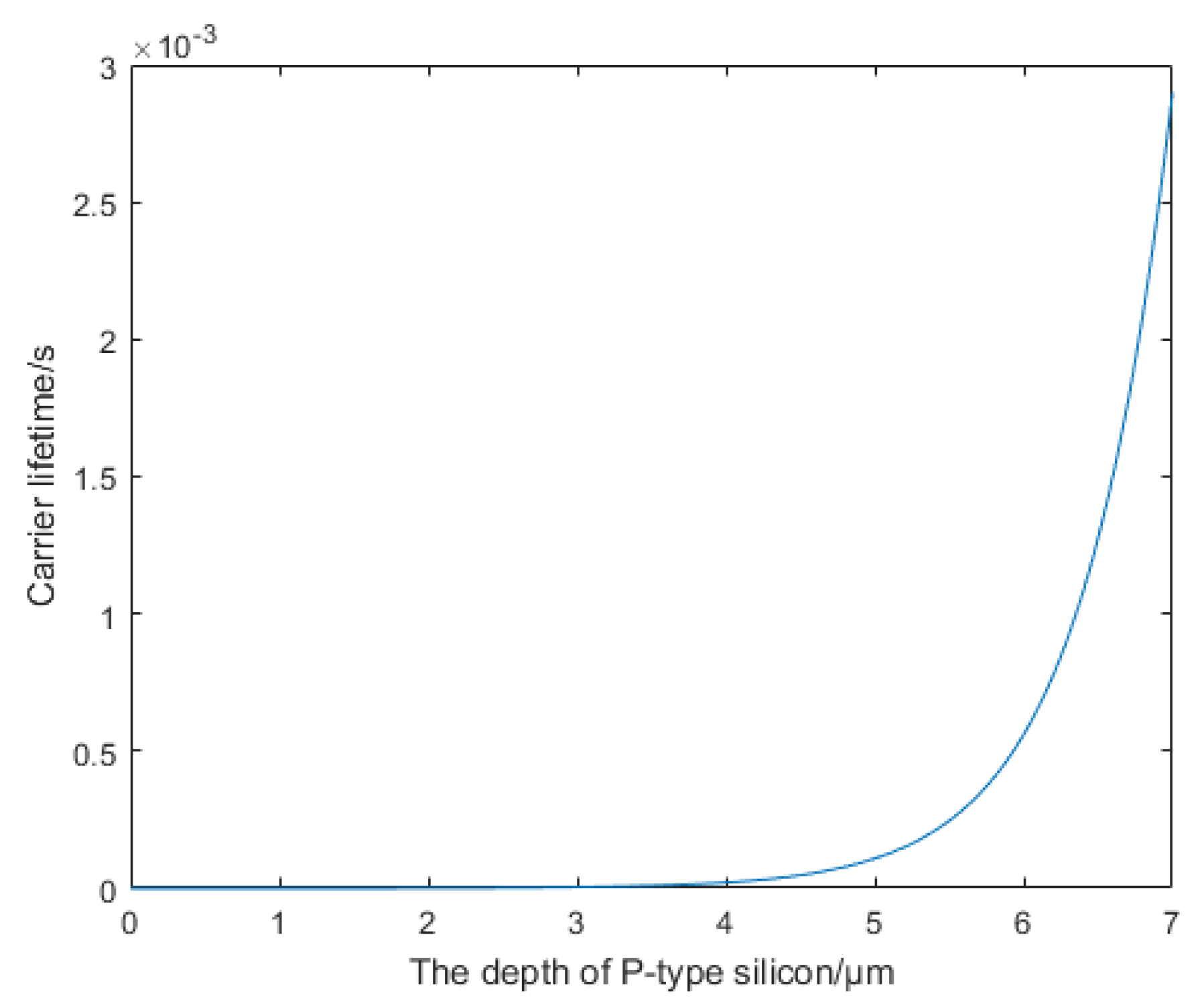
Figure 2.
The variation of minority carrier lifetime with depth in heavy exponential doping layers of different thicknesses under layered exponential doping structure: (a) The thickness of the heavy exponential doping layer is 0.1μm; (b) The thickness of the heavy exponential doping layer is 1μm.
Figure 2.
The variation of minority carrier lifetime with depth in heavy exponential doping layers of different thicknesses under layered exponential doping structure: (a) The thickness of the heavy exponential doping layer is 0.1μm; (b) The thickness of the heavy exponential doping layer is 1μm.
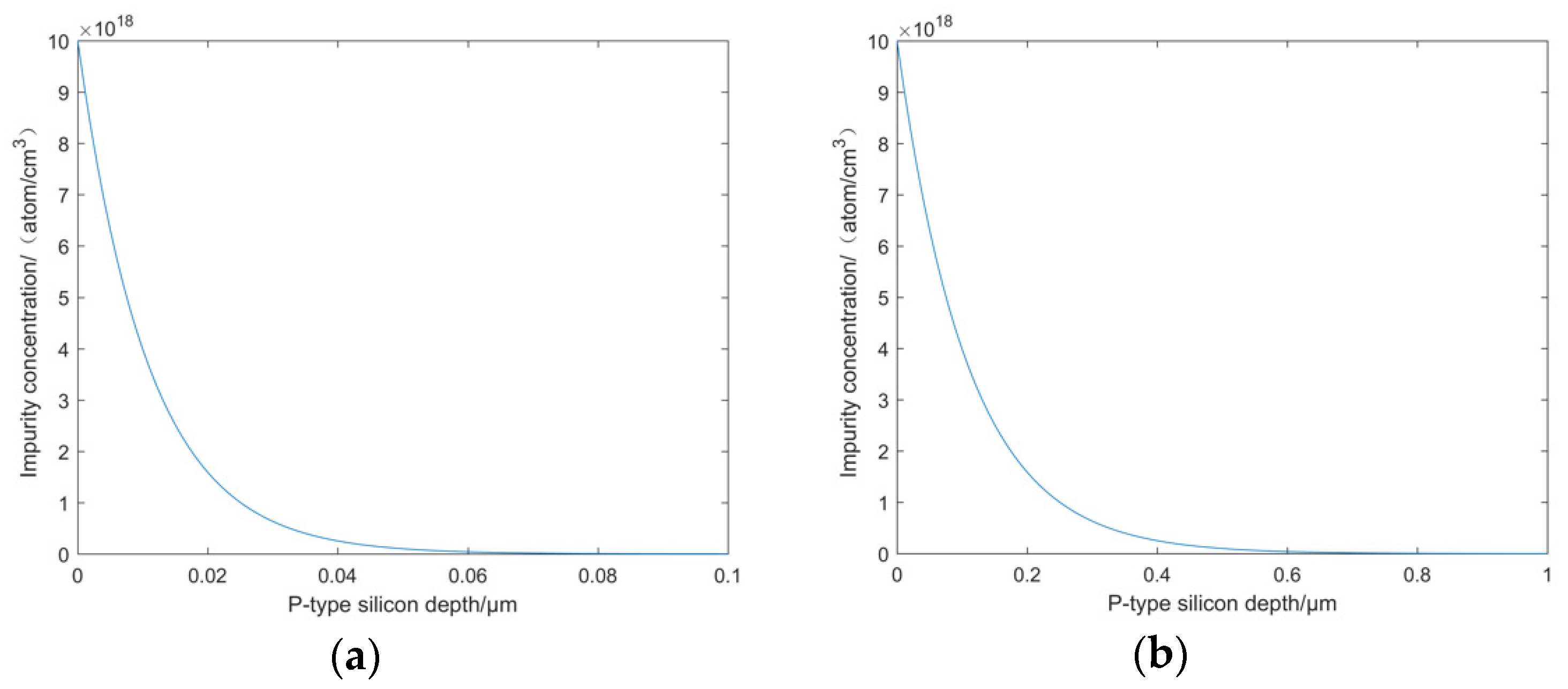
Figure 3.
Schematic diagram of electron multiplication layer structure and electron distribution in the 5×5 pixel region during uniform heavy doping
Figure 3.
Schematic diagram of electron multiplication layer structure and electron distribution in the 5×5 pixel region during uniform heavy doping
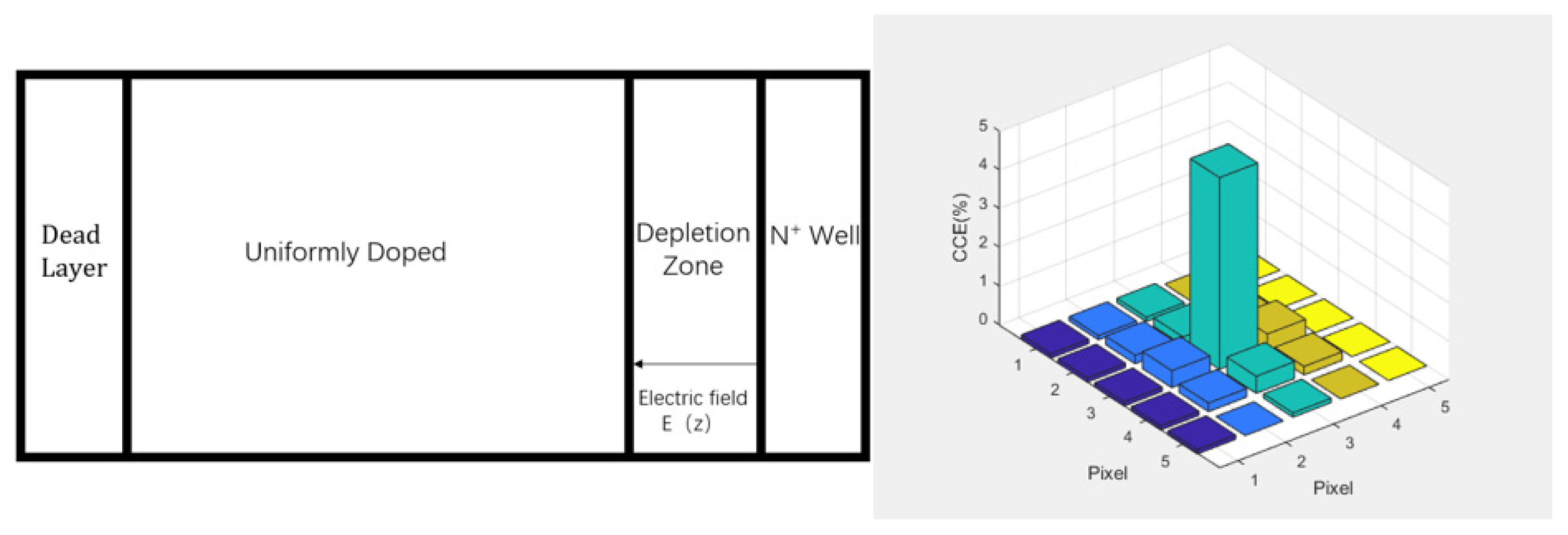
Figure 4.
Schematic diagram of electron multiplication layer with overall exponential doping and electron distribution in the 5×5 pixel region
Figure 4.
Schematic diagram of electron multiplication layer with overall exponential doping and electron distribution in the 5×5 pixel region
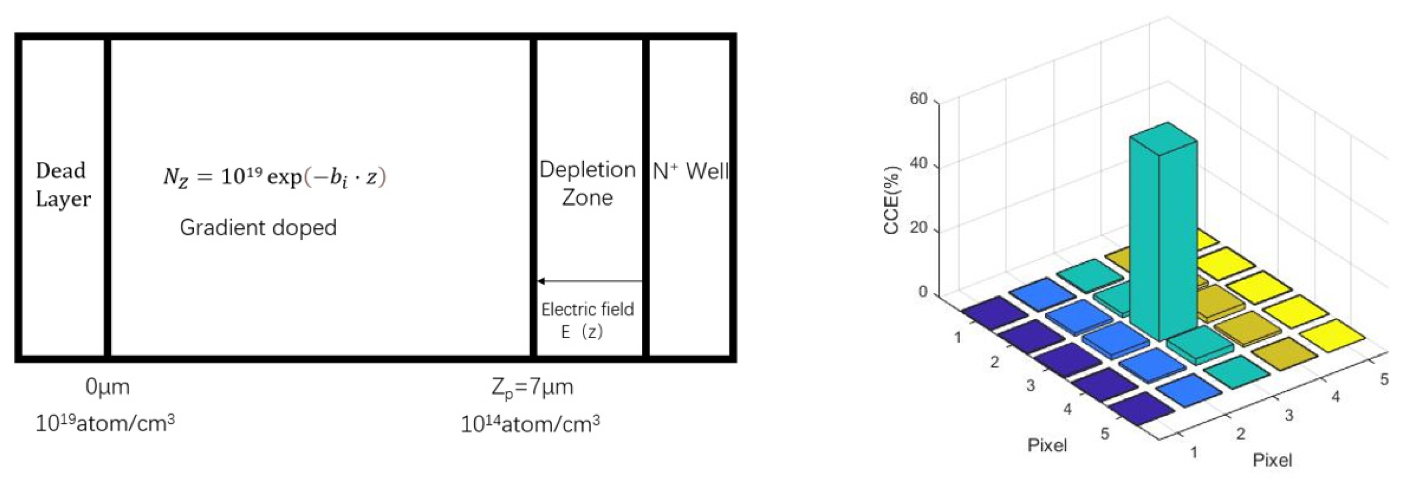
Figure 6.
Schematic diagram of the electron multiplier layer with the second layered exponential doping and the electron distribution in the 5×5 pixel region
Figure 6.
Schematic diagram of the electron multiplier layer with the second layered exponential doping and the electron distribution in the 5×5 pixel region
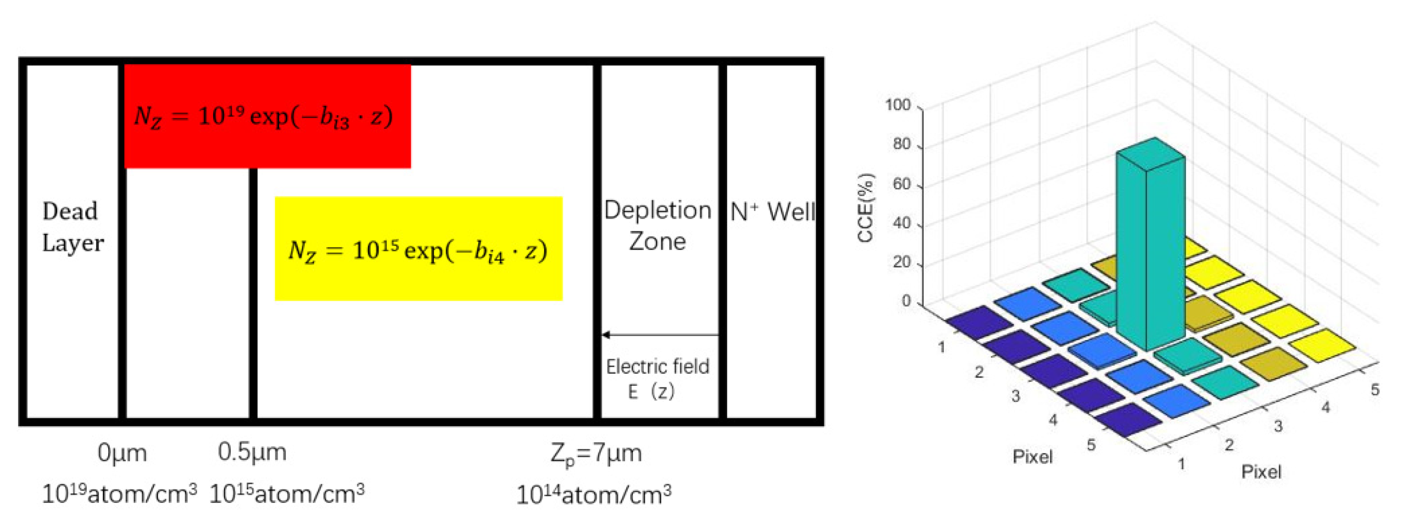
Figure 8.
Curve of impurity concentration with depth during ion implantation: (a) Thickness of heavy exponential doping layer is 0.1μm (b) Thickness of heavy exponential doping layer is 1μm Internal figure: curve of impurity concentration index with depth
Figure 8.
Curve of impurity concentration with depth during ion implantation: (a) Thickness of heavy exponential doping layer is 0.1μm (b) Thickness of heavy exponential doping layer is 1μm Internal figure: curve of impurity concentration index with depth
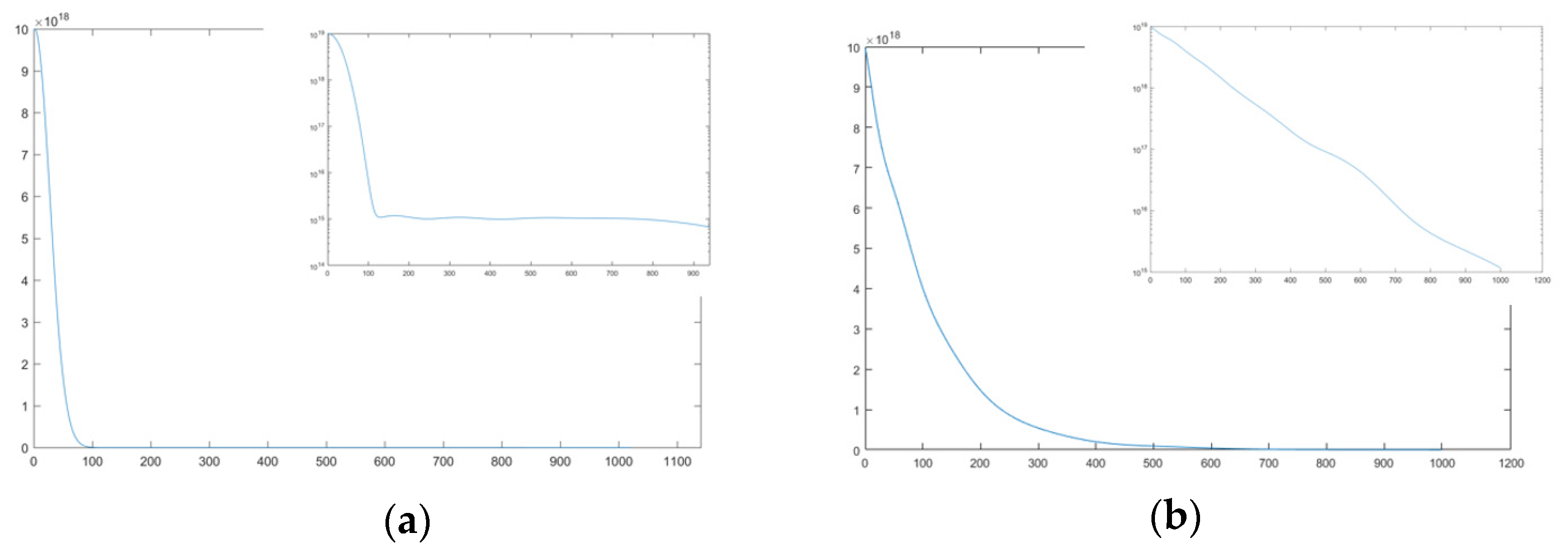
Figure 9.
Relation of electron energy loss rate with acceleration voltage
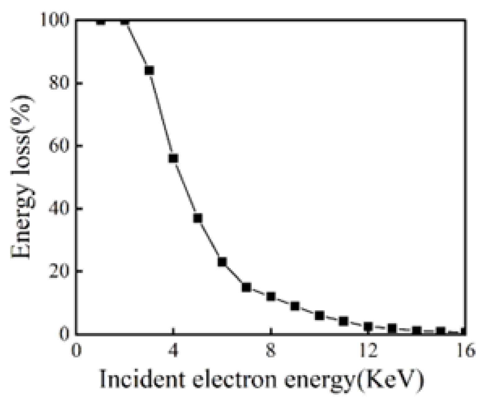

Table 1.
The injected dose and the corresponding Rp and ΔRp for the heavy exponential doping layer thickness of 0.1μm.
Table 1.
The injected dose and the corresponding Rp and ΔRp for the heavy exponential doping layer thickness of 0.1μm.
| Inject energy/keV | 15 | 28 | 44 | 60 | 80 | 116 | 195 | 290 | 407 |
|---|---|---|---|---|---|---|---|---|---|
| Inject dose/cm-2 | 4.7e20 | 4.5e20 | 2.5e20 | 1.7e20 | 1e20 | 7.8e19 | 2.1e19 | 1.2e18 | 5.4e17 |
| Rp/nm | 61.6 | 109.6. | 157.9 | 207.1 | 263.4 | 360.9 | 556.8 | 758.3 | 962.1 |
| ΔRp/nm | 25.6 | 39.4 | 53.1 | 58.5 | 69.1 | 83.4 | 103.2 | 118 | 141.5 |
Table 2.
The injected dose and the corresponding Rp and ΔRp for the heavy exponential doping layer thickness of 1μm.
Table 2.
The injected dose and the corresponding Rp and ΔRp for the heavy exponential doping layer thickness of 1μm.
| Inject energy/keV | 15 | 60 | 116 | 195 | 290 | 407 |
|---|---|---|---|---|---|---|
| Inject dose/cm-2 | 6.4e20 | 1.1e17 | 1.9e17 | 2.1e17 | 2.0e17 | 2.1e17 |
| Rp/nm | 61.6 | 207.1 | 360.9 | 556.8 | 758.3 | 962.1 |
| ΔRp/nm | 25.6 | 58.5 | 83.4 | 103.2 | 118 | 141.5 |
Table 3.
Resistivity and doping impurity concentration at different depths No.1: Thickness of heavy exponential doping layer is 0.1μm No. 2: thickness of heavy exponential doping layer is 1μm.
Table 3.
Resistivity and doping impurity concentration at different depths No.1: Thickness of heavy exponential doping layer is 0.1μm No. 2: thickness of heavy exponential doping layer is 1μm.
| Depth/μm | Resistivity/Ω.cm | Doping concentration/atom/cm3 | |
|---|---|---|---|
| No.1 | 0 | 9.01e-3 | 9.8e18 |
| 0.1 | 13 | 1e15 | |
| 0.2 0.3 0.4 0.5 0.6 0.7 0.8 0.9 |
13.8 14 15.1 15.3 15.9 16.2 16.5 17.3 |
9.7e14 9.4e14 9e14 8.7e14 8.5e14 8.2e14 8e14 7.6e14 |
|
| No.2 | 0 | 9e-3 | 9.8e18 |
| 0.1 0.2 0.3 0.4 0.5 0.6 0.7 0.8 0.9 |
1.7e-2 3.4e-2 5.9e-2 0.1 0.202 0.43 0.95 2.5 5.3 |
4e18 1.5e18 6.2e17 2.5e17 1e17 3.9e16 1.6e16 6.2e15 2.3e15 |
Table 4.
Charge collection efficiency of two samples at 3KV~8KV acceleration voltage
| Accelerating voltage/kV | 3 | 4 | 5 | 6 | 7 | 8 |
|---|---|---|---|---|---|---|
| No.1 CCE/% | 84.25 | 85.44 | 86.29 | 86.97 | 87.33 | 87.32 |
| No.2 CCE/% | 71.84 | 71.96 | 72.34 | 72.84 | 73.42 | 73.5 |
Disclaimer/Publisher’s Note: The statements, opinions and data contained in all publications are solely those of the individual author(s) and contributor(s) and not of MDPI and/or the editor(s). MDPI and/or the editor(s) disclaim responsibility for any injury to people or property resulting from any ideas, methods, instructions or products referred to in the content. |
© 2023 by the authors. Licensee MDPI, Basel, Switzerland. This article is an open access article distributed under the terms and conditions of the Creative Commons Attribution (CC BY) license (http://creativecommons.org/licenses/by/4.0/).
Copyright: This open access article is published under a Creative Commons CC BY 4.0 license, which permit the free download, distribution, and reuse, provided that the author and preprint are cited in any reuse.


