1. Introduction
Since Dr. Peter Grasher proposed the concept of satellite solar Power Station (SPS) [
1,
2,
3], radio energy transmission technology, especially Microwave Wireless Power Transfer (MWPT) technology, has gradually attracted people's attention.
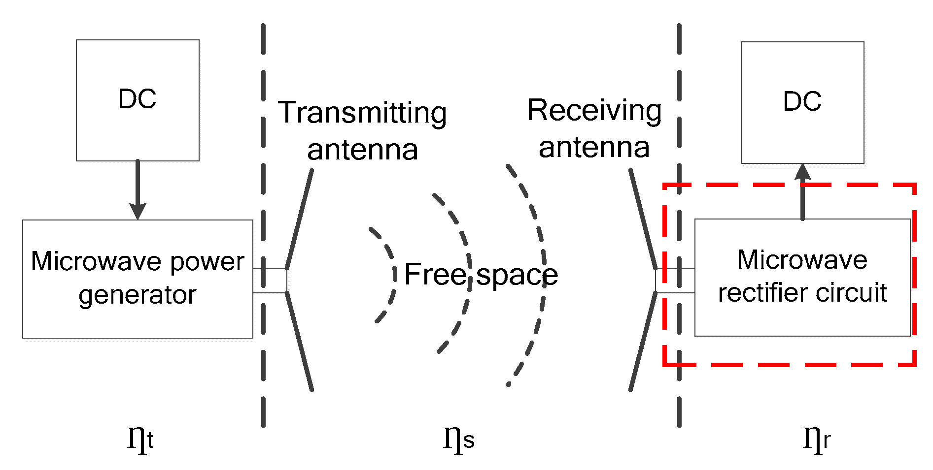
Figure 1 shows the MWPT schematic diagram. Due to the use of 300MHz-300GHzAs the carrier of energy transmission, MWPT has the advantages of long transmission distance and large transmission power compared with other wireless transmission methods [
4,
5,
6]. Of course, MWPT technology also has some shortcomings. Firstly, the overall energy conversion efficiency of DC-DC in MWPT system is still at a low level with the current technological level. Although the energy conversion efficiency of DC-RF at the transmitter and RF-DC at the receiver can reach more than 70% under ideal conditions, However, due to the influence of various factors such as antenna performance and transmission environment during electromagnetic wave space transmission, the power Pin (dBm) reaching the receiving end is extremely unstable and has a wide dynamic range [
7].When the input power changes, the nonlinearity of the rectifier device will correspondingly change the impedance in the input terminal, which leads to an impedance mismatch and greatly reduces the rectification efficiency [
8]. Therefore, many scholars have focused on the wide dynamic rectification technology. Most of the current wide dynamic rectification technology use multi-channel technology. For example, some scholars have designed a two-way adaptive control rectifier circuit by the sensitivity of MOSFETs to voltage. The power operating range of the circuit was broadened by switching the field-effect tube control circuit in two states, namely, series and parallel [
9,
10,
11]. Some scholars have also used microwave passive networks, such as non-uniform Wilkinson power dividers, to fully utilize the rectification capability of both high and low power branches, thus broadening the overall rectification capability of the circuit [
12,
13,
14,
15]. Based on the two-way microwave rectifier circuit, the research team of South China University of Technology introduced a third microwave rectifier circuit. The energy reflected from the first two branches due to impedance mismatch was fed to the third rectifier branch through a directional coupler, which significantly broadened the overall power dynamic range of the three-way output [
16,
17,
18,
19].
The non-uniform power distribution or automatic power distribution can effectively broaden the power dynamic range of microwave rectifier circuits and improve the stability of rectification efficiency of microwave rectifier circuits in the case of unstable spatial transmission. However, since each rectification branch in these two methods is non-uniform, the DC voltage at the output terminal of each branch is different and cannot be directly connected in parallel to charge the battery. A complex power electronic converter circuit (boost or buck circuit) needs to be introduced to adjust the output voltage of each branch to be consistent before parallel output. This results in additional power loss and is not conducive to DC power synthesis at the output load terminal. In order to solve this problem, it becomes necessary to study multi-channel rectifier circuits with consistent output voltages. Such a circuit will not only broaden the power dynamic range of the rectifier circuit, but also enable the output voltage to be directly used for battery charging in parallel, avoiding complex power electronic conversion at the load side that will influence the wireless charging efficiency. Therefore, this circuit has high practical value. To obtain a wide dynamic rectifier circuit that facilitates DC power synthesis at the output terminal, a four-channel wide dynamic microwave rectifier circuit has been designed in the paper for the shortcomings of the traditional wide dynamic rectifier circuit with uneven output voltage. The four rectifier branches shared the same load at the output terminal, allowing the rectifier circuit to have an RF-DC conversion efficiency greater than 50% over the input power range from 12mW to 274mW, widened by 274% compared to a single channel. Not only the advantages of multi-channel technology with wide dynamics were retained, but also the output voltage was highly consistent and could be directly output in parallel without complex power electronics conversion. To a certain extent, the output power and the practicality of this energy harvesting system have been increased. Finally, a complete MWPT experimental system was built, and the experimental results proved the feasibility of the scheme.
2. Analysis of the Principle of the Circuit
2.1. Combination Form of Multi-Channel Rectification
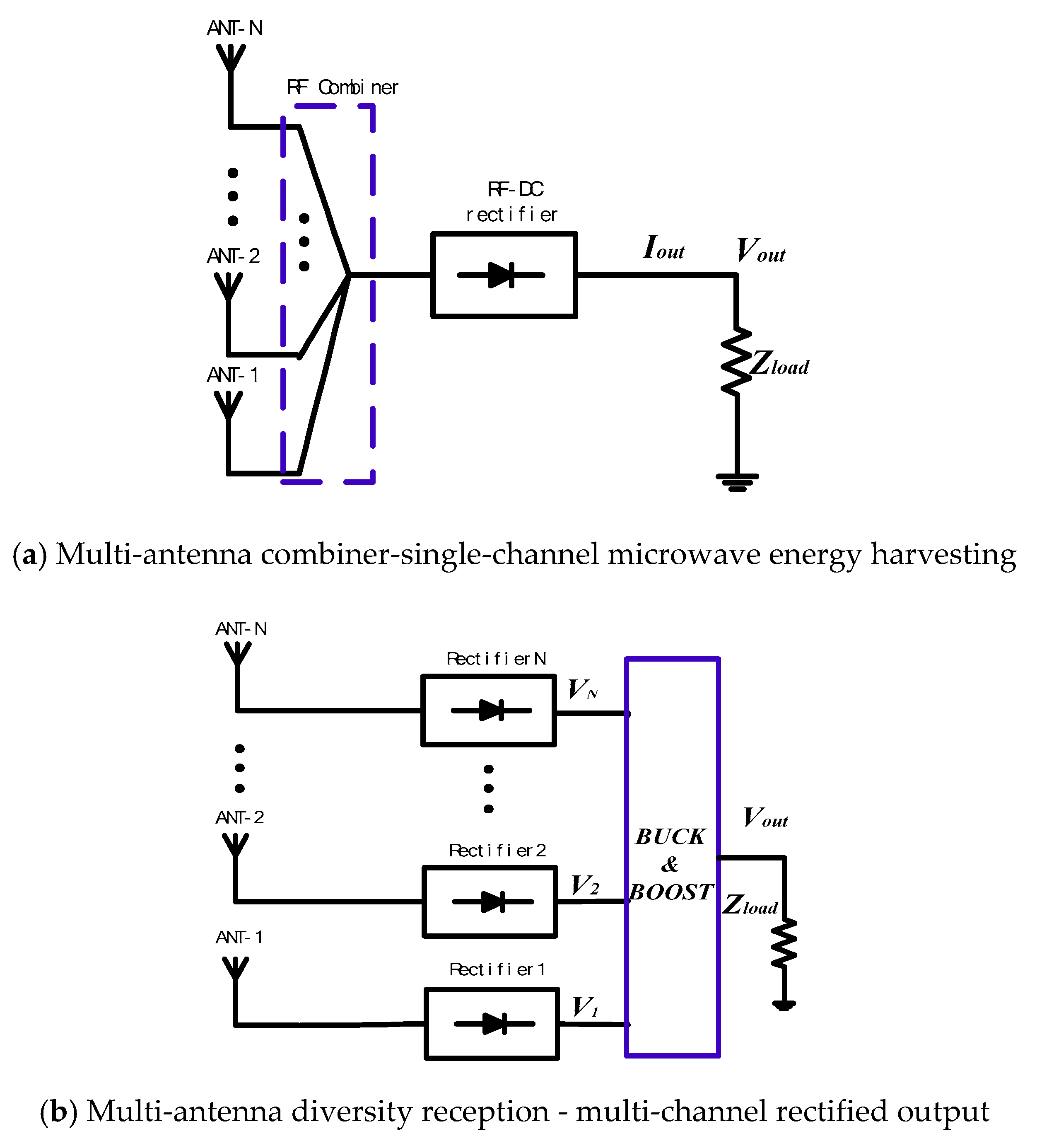
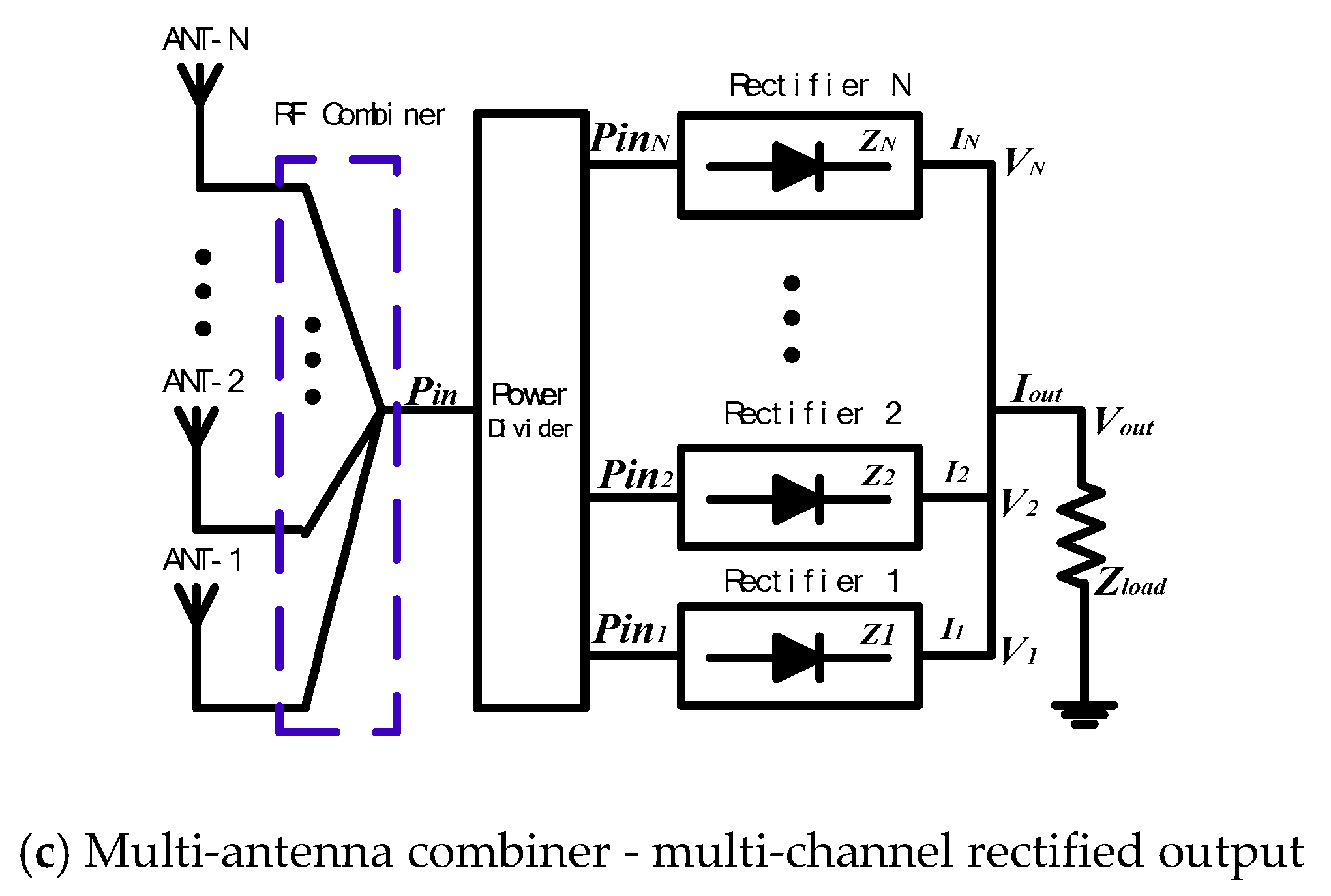
The combined form of the multi-channel rectifier circuit is shown in
Figure 2.
Figure 2a shows that the electromagnetic waves in space were collected by each antenna unit of the antenna array, transformed into RF power all the way through the combiner, delivered to a conventional single-channel rectifier circuit, and then converted into DC voltage output at the load side. Although the use of antenna arrays allowed for greater input power, a conventional single channel was used in the rectifier circuit, which had a narrow power dynamic range. In
Figure 2b, multiple antennas were used for diversity reception, and each antenna unit corresponded to an independent rectifier circuit, which can ensure that multiple channels could harvest energy simultaneously with a wide power dynamic range. However, since the antennas were located in different locations in space, it was impossible to guarantee that each antenna got the same power. Even if the performance of each rectifier branch was the same, it was difficult to make each output voltage consistent, and the output side should be equipped with a boost or buck circuit in order to output stable voltage in parallel. These circuits themselves introduced losses that influenced the efficiency of the DC synthesis output at the load terminal. In this paper, the form of
Figure 2c was used. The electromagnetic energy received by each unit of the antenna array was combined and input to the quartile power distribution network, and output to four identical voltage doubling rectifier circuits respectively. Such a multi-channel rectification technology not only increased the power capacity of the rectifier circuit and broadened the power dynamic range, but also enabled each circuit to obtain a high and consistent output voltage. In this way, the outputs can be directly connected in parallel for battery charging, avoiding the need for complex power electronic transformations and thus maintaining stable DC synthesis output efficiency.
As shown in
Figure 2c, the RF power obtained from each antenna unit of the high-gain antenna array was combined into one RF power P
in input to the rectifier circuit through the combiner, thus a good input power could be obtained. At the output side, the output voltage of each branch was equal and all rectifier branches shared the same load
Zload. In this way, not only can a larger DC output power be obtained, but it could also be used to charge the battery directly. The characteristics of the circuit can be expressed by the following equation:
In fact, for each rectifier branch, the output impedance was equal. According to the above formula, the DC output power at the load can be derived as:
The overall efficiency of the circuit can be expressed as:
2.2. Mechanisms for Achieving Wide Power Dynamic Range
Taking a four-channel microwave rectifier circuit with equal power division as an example, this paper has analyzed the effect of multi-channel rectification on the power dynamic range by establishing an approximate mathematical model based on the interval. It was still assumed that the power dynamic range of a single rectifier branch was approximated as a equilateral triangle. Since it was 1 divided into 4 uniform distribution, we could assume each branch input power
P1=
P2=
P3=
P4=
x, then the total input power P
in = 4
x. As shown in
Figure 3, the single branch rectification efficiency greater than 50% was in the interval of [1.5W,2.5W] with a dynamic range of 1W. All four rectifier branches had the same form. The power dynamic range of the combined four-channel rectifier circuit was shown in the Figure, and its total efficiency above 50% was between [6W,10W] with a dynamic range of 4W, which was four times that of the single rectifier branch.
Ideally, multi-channel rectification technology can broaden the power dynamic range of RF-DC energy conversion, the fundamental reason of which is that it can broaden the power "capacity" of the rectifier circuit. That is, it allows more RF power to be converted to DC energy through the rectifier circuit at the same time.
3. Simulation and Design of the Circuit
3.1. Design of Single-Circuit Microwave Rectifier Circuit
Before designing the four-channel rectifier circuit, the single-channel microwave rectifier circuit first needs to be designed on the simulation software. The HSMS286C voltage doubling rectifier structure was used, and a low-pass filter with a simple structure was used as the DC filter. After simulation optimization, the structure of a single rectifier branch was obtained as shown in
Figure 4. The dielectric constant of the plate was
εr and the thickness of the plate was H. At the operating frequency of 2.45 GHz, the microstrip antenna width was
W1, the length of front impedance matching series branch was
a1, the parallel branch length was
a2, the length of rear impedance matching series branch was
a3, the length of parallel short circuit branch was
a4,
a5, the series inductor was
L1, the length of DC filter series branch was
a6, the parallel branch length was
a7, and the load was
Zload1. After optimization, the parameters of each circuit are shown in
Table 1.
In order to better analyze the variation law of output DC voltage with input power, the parameters of individual rectifier branch
S11 and the variation curve of output DC voltage
Vout1 with input power
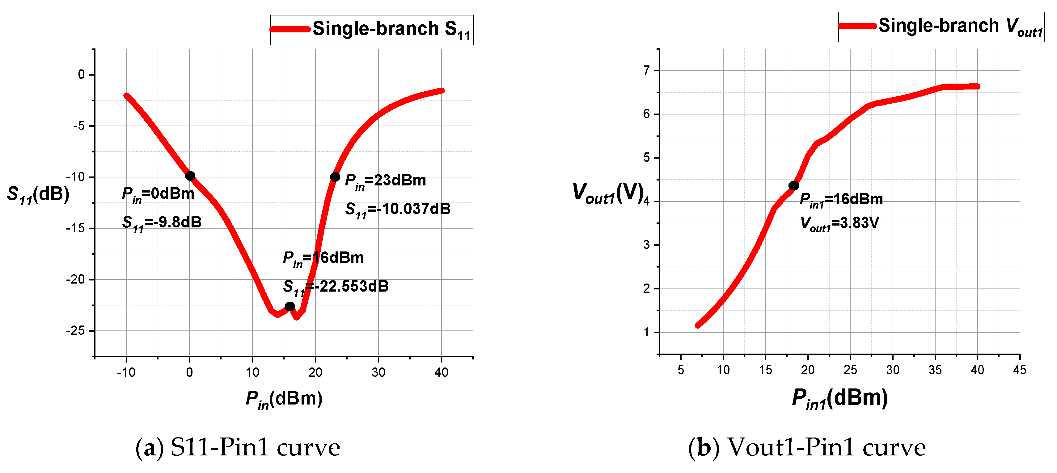
Pin1 were obtained by software simulation. From the S curve in
Figure 5a, it can be seen that when
Pin1 was between the power interval of 0dBm to 23dBm,
S11 was less than -10dB, indicating that the branch was in a better impedance matching state in this interval. And from the output voltage curve in
Figure 5b, it can be seen that as the input power gradually increased from
Pin1 = 5dBm, the slope of the voltage increased with power, and the output voltage
Vout1 also gradually increased. When
Pin1=16dBm, the slope of the increment of
Vout1 was maximum, which was 3.8V. When the input power
Pin1 exceeded 20dBm, although the output voltage
Vout1 was still increasing, it increased slowly and gradually entered a stable status. Since the load was constant, it indicated that the increased input power did not bring enough output power. This was because the diode was reversed breakdown, which caused additional power loss, and the RF-DC rectification efficiency started to drop.
Let the input power of a single rectifier branch be
Pin1 (unit was dBm) as a variable, the real part of the output voltage was
Vout1 (unit was V),
Zload1 was the load impedance of the branch, the single microwave rectifier branch RF-DC conversion efficiency
PCE1 (Power Conversion Efficiency, PCE1) could be calculated according to the following formula:
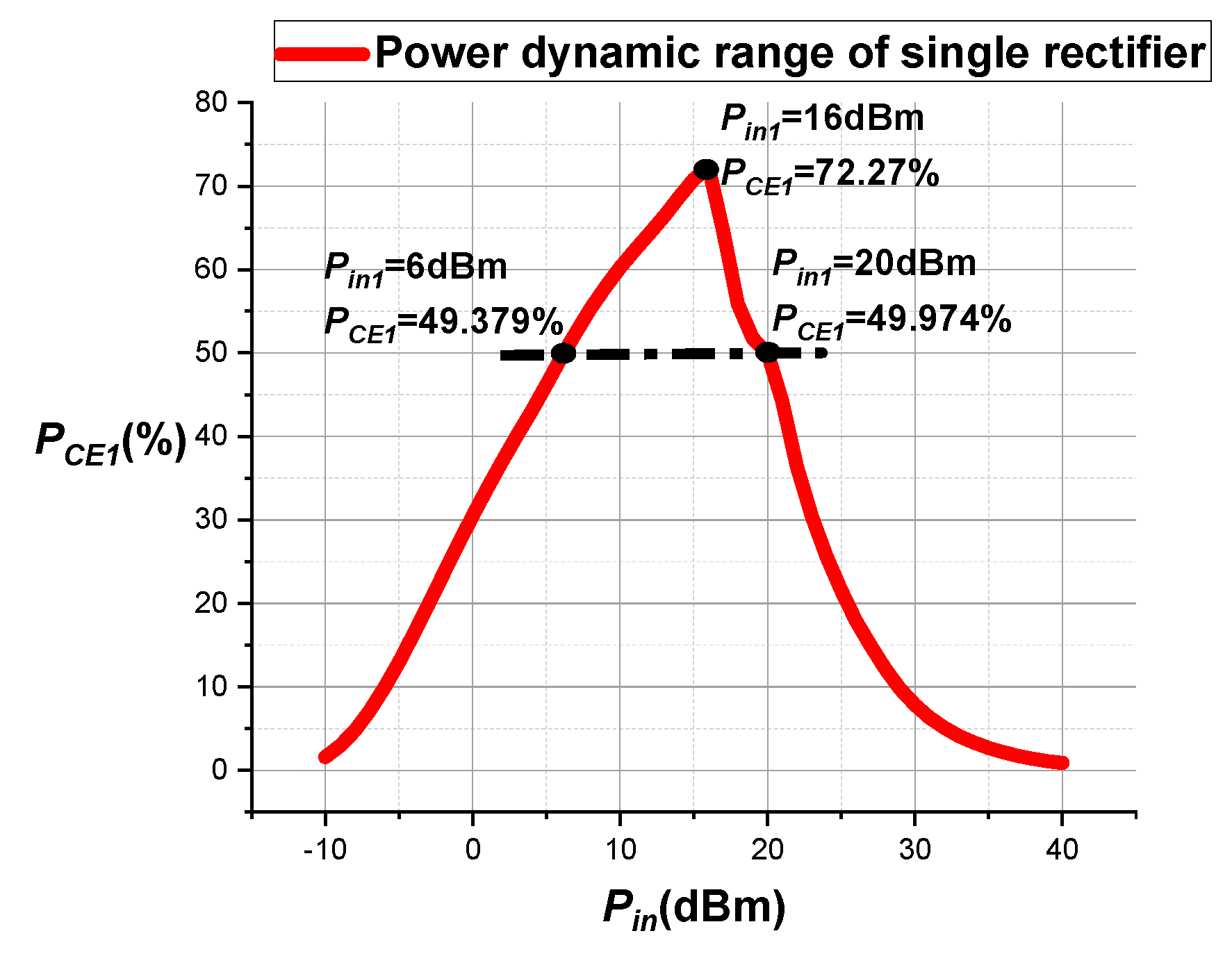
To further illustrate the power dynamic range of this rectifier, the efficiency-input power dynamic range curve for a single rectifier branch was plotted in
Figure 6. The curve shows that the maximum rectification efficiency of a single rectifier branch appeared when the input power
Pin1 = 16dBm, the maximum RF-DC conversion efficiency at this time was 72.27%. It can also be seen from the curve that for a single branch input power
Pin1 between 6dBm to 20dBm (about 14dBm power dynamic range), the RF-DC conversion efficiencies were all greater than 50%.
3.2. Design of Quadratic Power Division Network
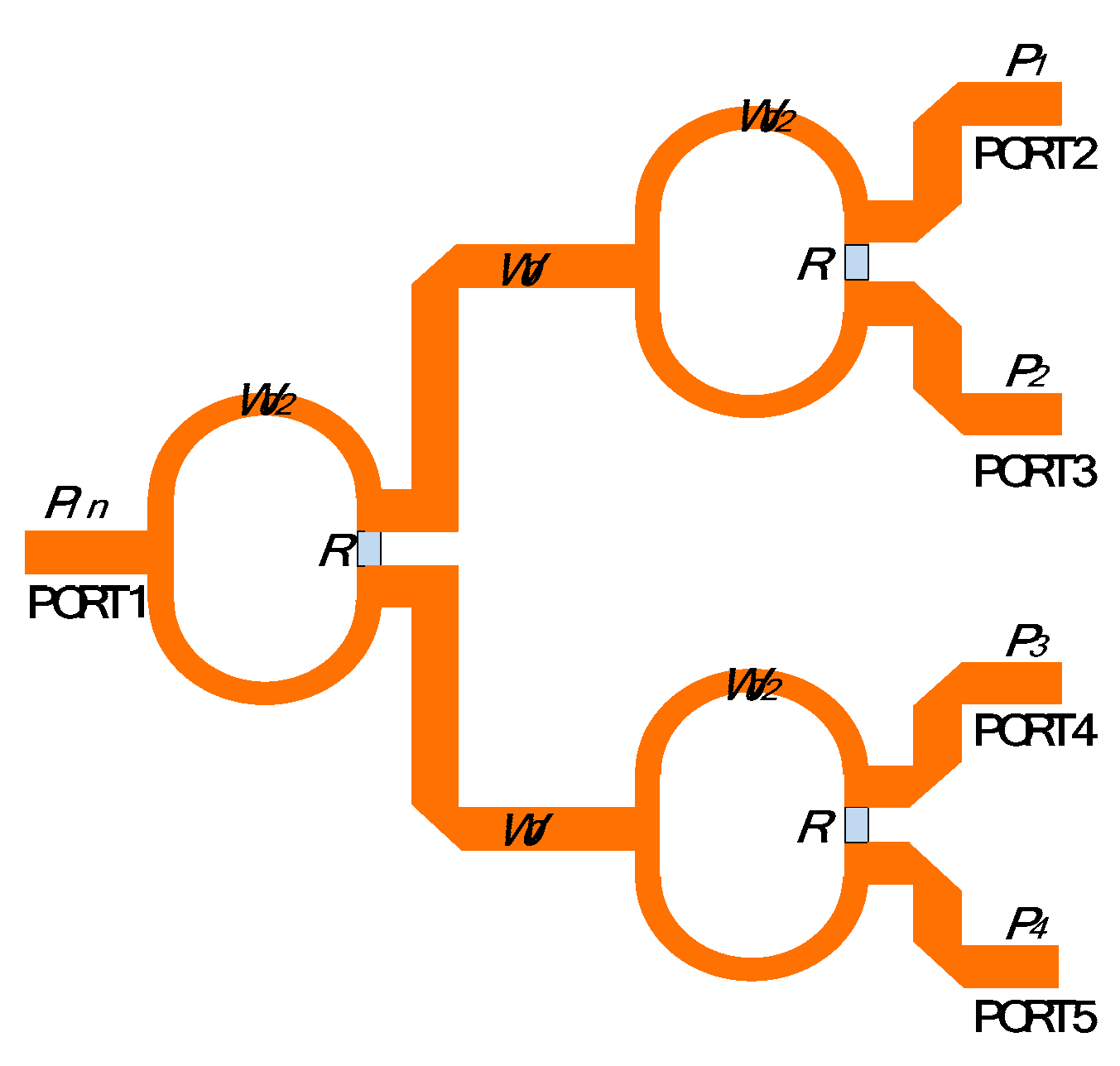
According to the principle of Wilkinson power divider, when certain conditions are met, the power divider can divide the input RF power equally into two branches for output. By nesting three such equally divided Wilkinson power dividers together, a four-equivalent network was obtained. As shown in
Figure 7, the board material dielectric constant was
εr, the thickness of the plate was H, the width of the power divider transmission line was
W0, the width of the 1/4 wavelength converter was
W02, and the isolation resistance was R. Simulation and optimization of this power-division network were carried out to obtain the parameters of the power-division network circuit, as shown in
Table 2.
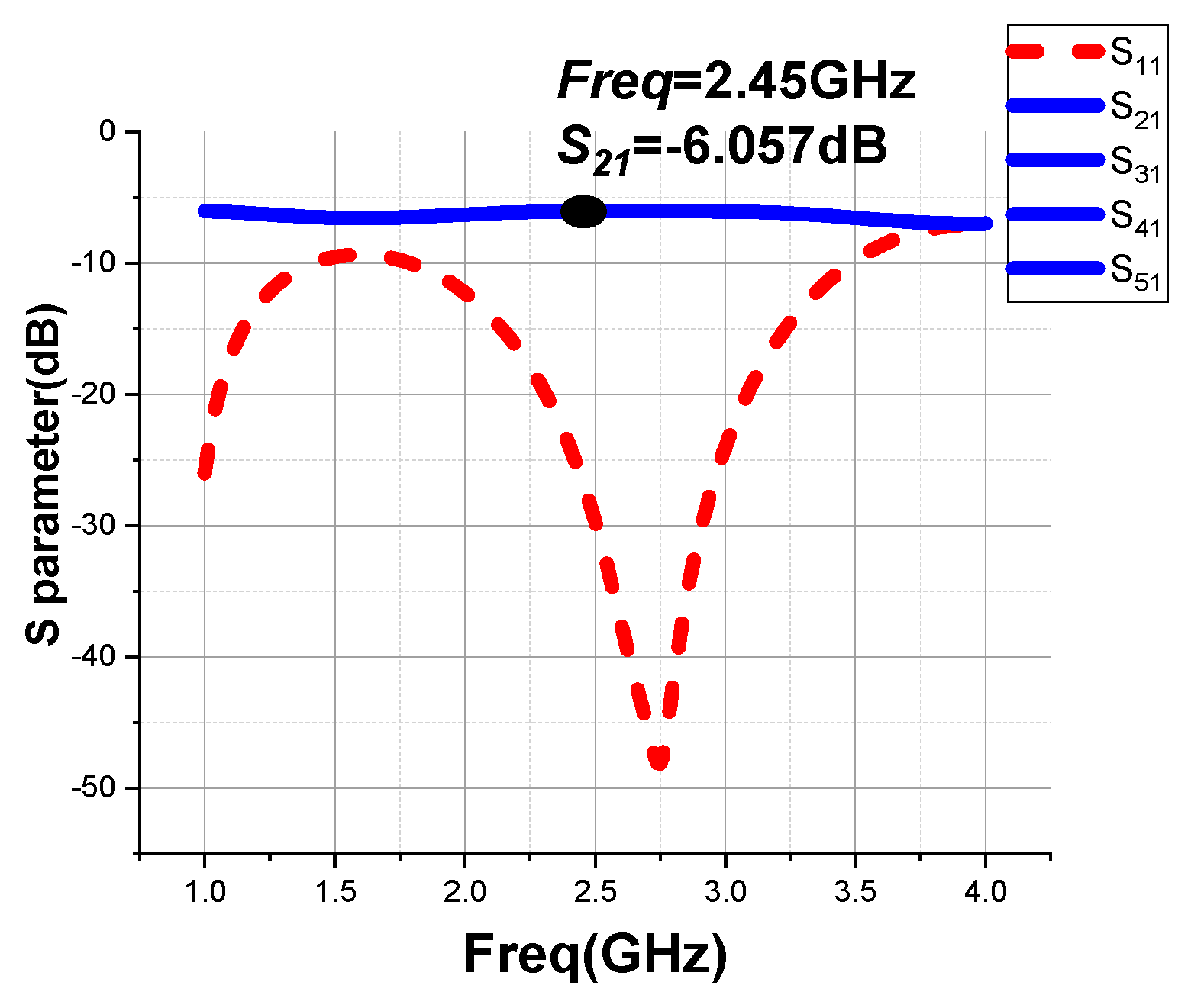
The S parameters of the designed four-equivalent Wilkinson power divider network were simulated, and the S-parameter characteristic curves of each port are shown in
Figure 8. As can be seen in
Figure 8, the power-division network S11 = -26.5 dBm at 2.45 GHz and maintains impedance matching over a wide bandwidth range. Each output port
S21、
S31、
S41、
S51 were highly overlapping, and
S21=
S31=
S41=
S51≈-6dB at 2.45GHz. This indicated that the power at each output port was 1/4 of the input power
Pin, and the RF input power obtained from the antenna by the rectifier circuit had been evenly divided into four equal-sized portions.
3.3. Overall Circuit Performance Optimization and Analysis
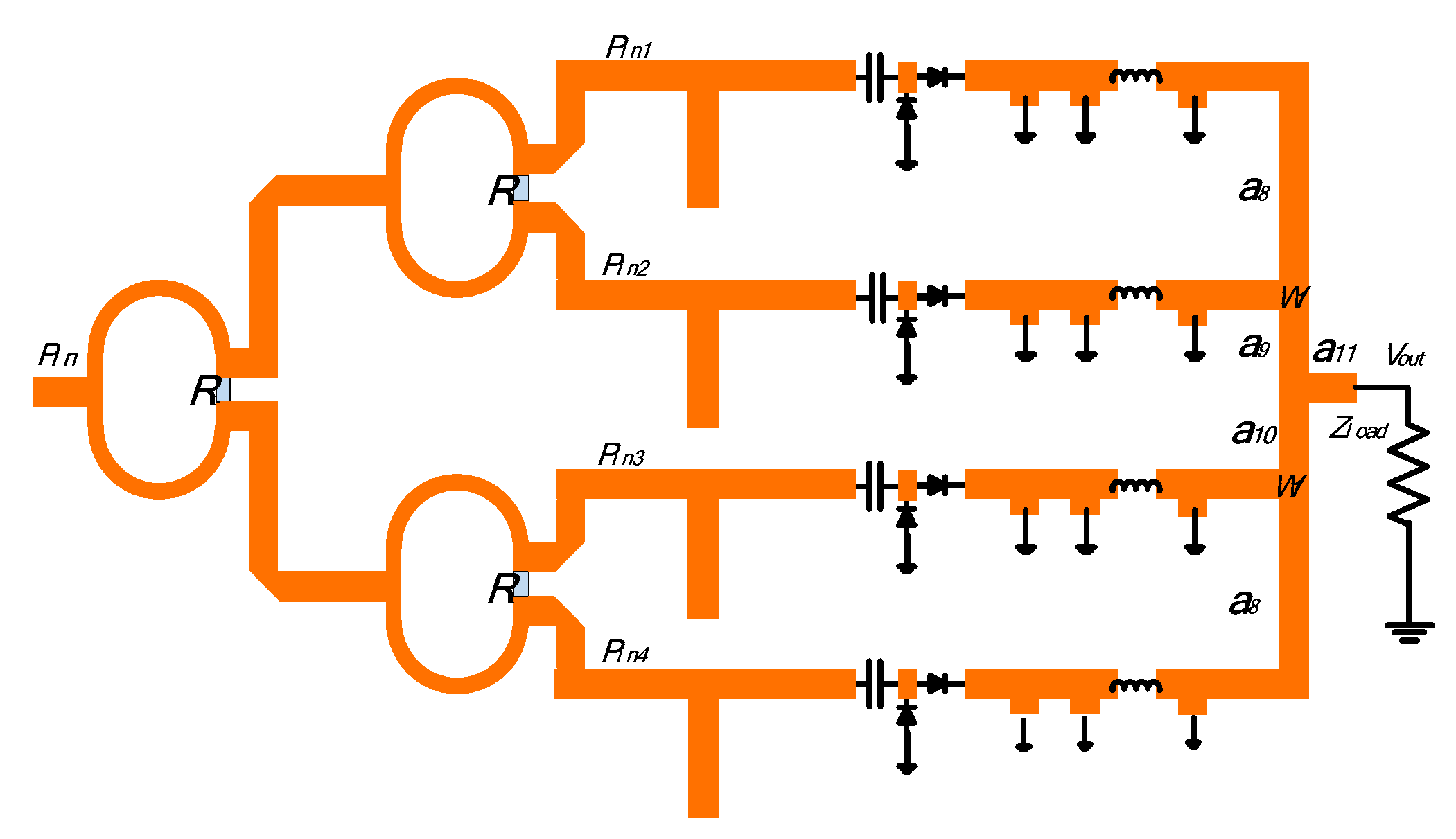
As shown in
Figure 9, four identical single rectifier circuits were connected to the four output interfaces of the four-equivalent power divider network, and the whole four-channel microwave rectifier circuit was simulated and optimized. Its general parameters were consistent with those of individual debugging. Due to the change of parameters after the circuit combination, the microstrip line length at the load side and the parameters of the load
Zload itself needed to be optimized, and the optimized circuit parameters are shown in
Table 3.
The
S11 parameter of the whole rectifier circuit and the variation curve of the output DC voltage
Vout with the input power
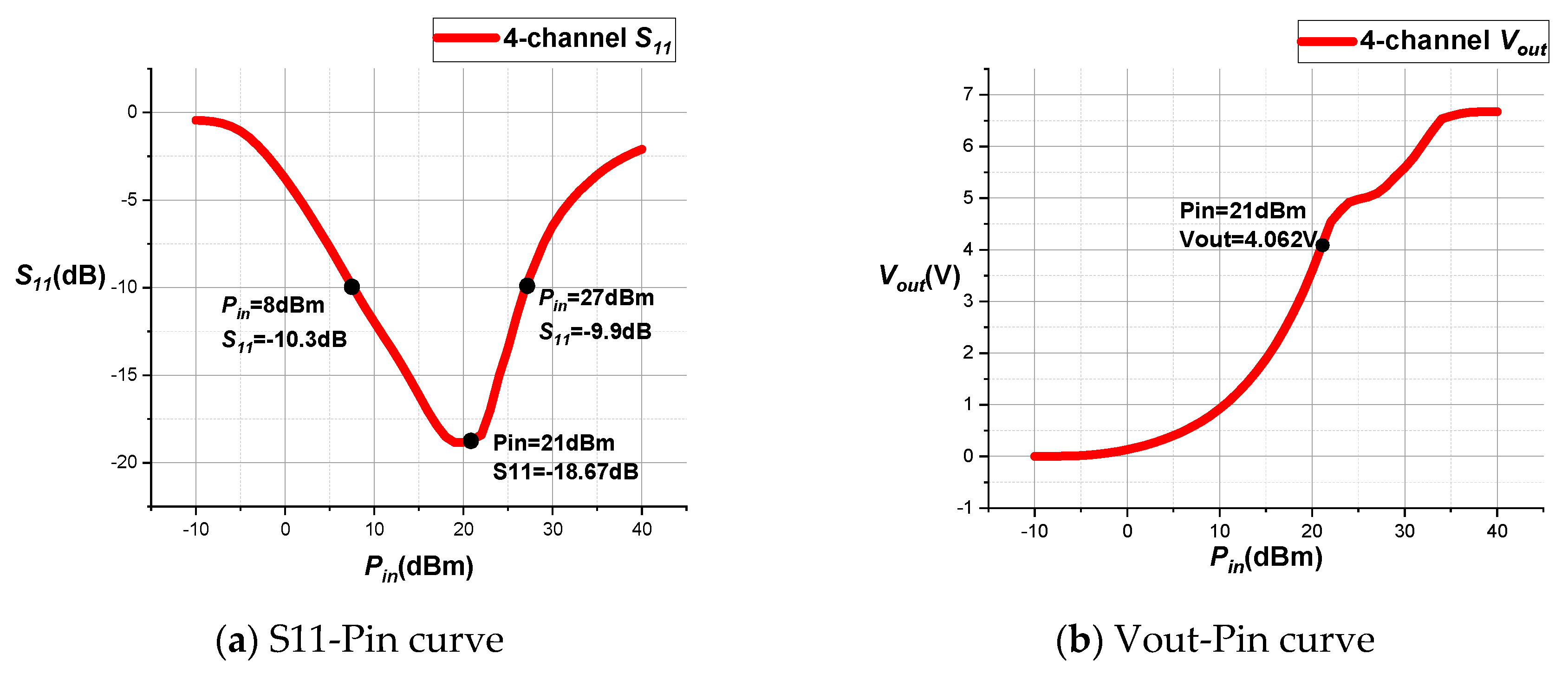
Pin were obtained by software simulation. From the S curve in
Figure 10a, it could be seen that when
Pin was between the interval of 8dBm to 27dBm, S11 was less than -10dB, indicating that the branch was in a better impedance matching state in this interval. When the input power
Pin = 21dBm,
S11= -18.67dB. And as can be seen from the output voltage curve in
Figure 10b, as the input power gradually increased from
Pin = -10dBm, the slope of the voltage increased with power, and the output voltage
Vout gradually increased. When
Pin = 21dBm, the slope of the increment of
Vout was maximum, at which time the output DC voltage was 4.062V. When the input power
Pin exceeded 21dBm, the output voltage
Vout increased slowly and gradually entered a stable status.
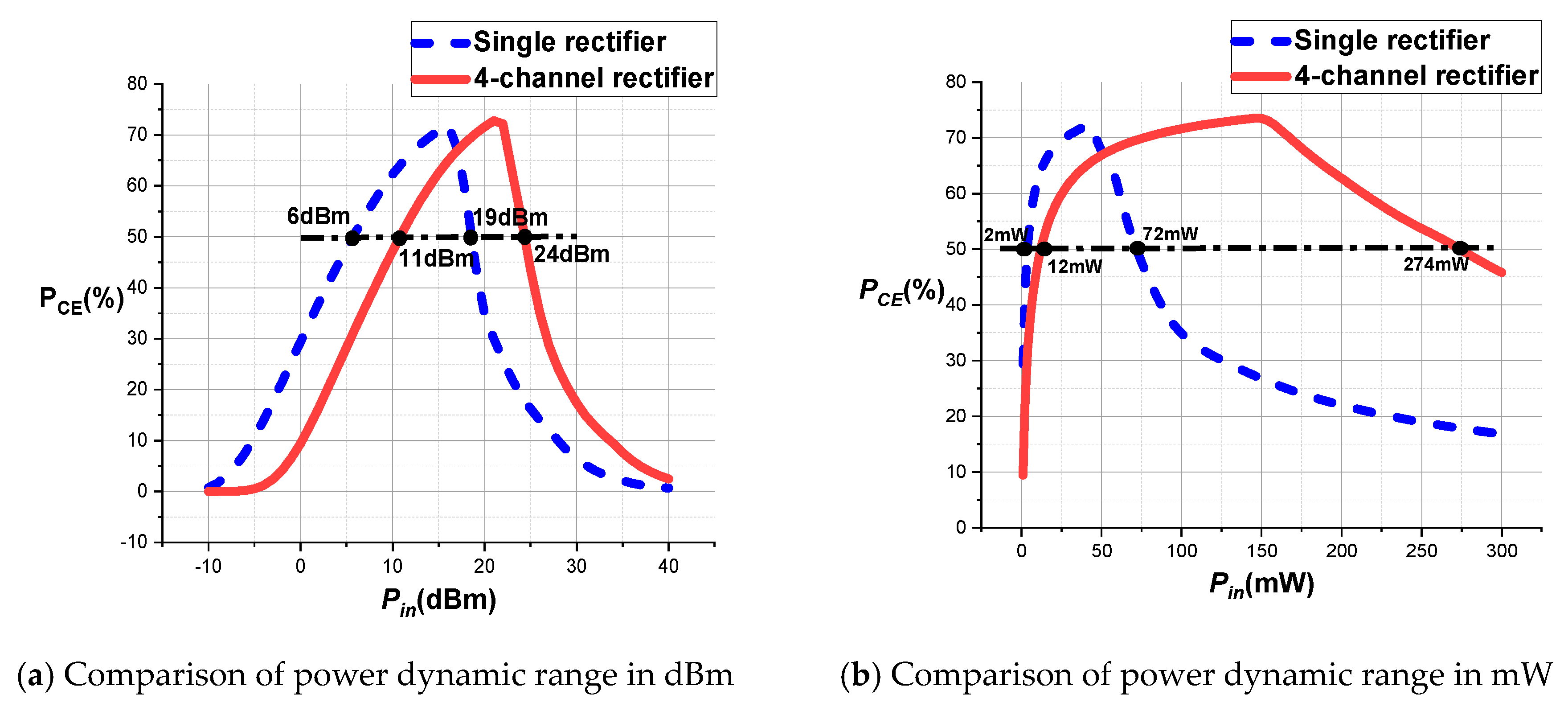
In this paper, the power dynamic range of the combined four-channel microwave rectifier circuit was compared with the power dynamic range of a single rectifier branch in
Figure 11.
Figure 11a shows a comparison of the power dynamic range in milliwatts. It can be seen that the RF-DC conversion efficiency of the designed four-channel microwave rectifier circuit with a shared load was greater than 50% when the input power
Pin was in the range of 11dBm to 24dBm (a total range of 13dBm). Compared to the power from 6dBm to 19dBm in the single-channel rectifier, the range was not significantly broadened. However, the power capacity of the entire rectifier circuit was increased, making the rectifier circuit adapt to a wider input power range. If the input power
Pin is converted into milliwatts, it can be seen that the RF-DC conversion efficiency of the four-channel rectifier is greater than 50% in the range of 12mW to 274mW (a total range of 262mW), which is much wider than the dynamic power range of 2mW to 72mW (only 70mW) for a single-channel microwave rectifier circuit.
4. Experimental Verification
4.1. Microwave Rectifier Circuit Conduction Experiment
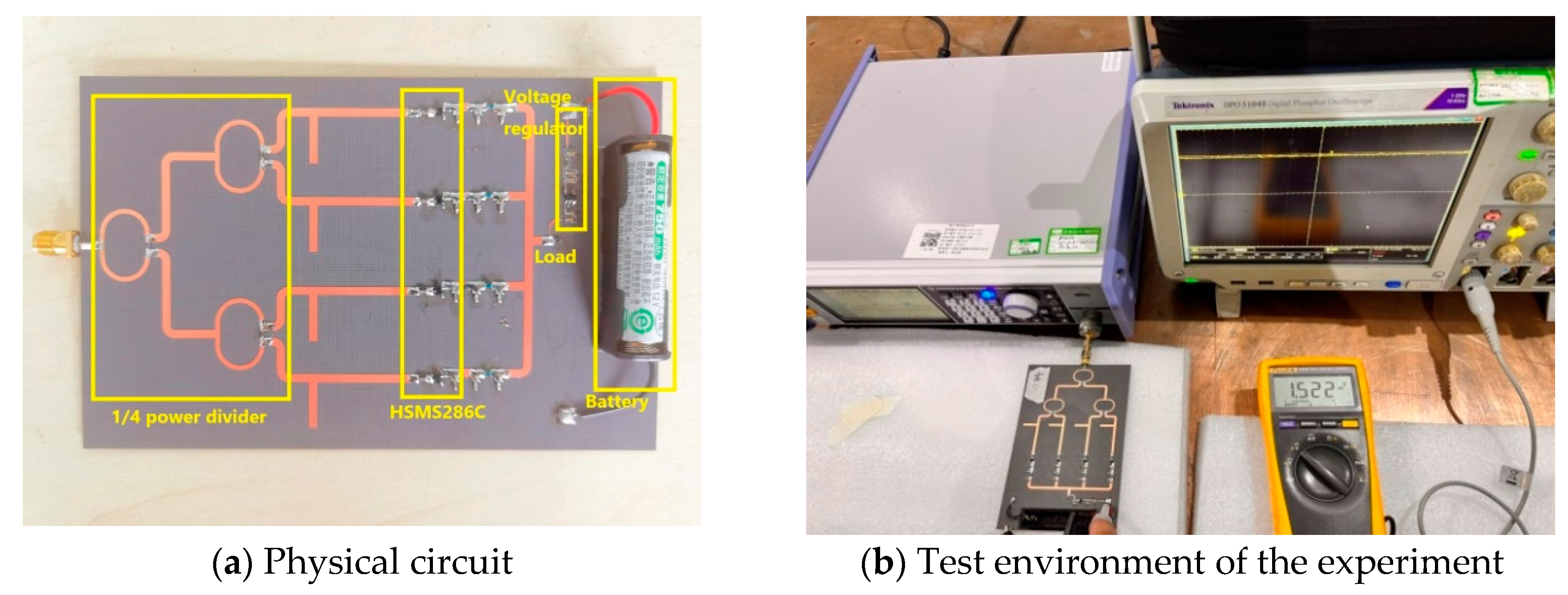
The rectifier circuit was physically fabricated according to the circuit parameters of the simulation design, as shown in
Figure 12. Due to the uncertainty of spatial transmission, the input power
Pin of the rectifier circuit could not be guaranteed to be constant. Therefore, the output voltage at the load side could also not be guaranteed to be a constant value. The charging of NiMH batteries generally requires a constant voltage to ensure safety. Therefore, a 1.5V regulator circuit was set up at the output, and a battery box was fixed on the circuit board. For wireless charging, a NiMH battery with a charging voltage of 1.5V could be loaded, with the positive terminal of the battery connected to a constant voltage output and the negative terminal grounded. Closed-loop conduction experiments were conducted on the designed circuit, and an RF signal generator was used as the microwave source. By adjusting the transmitting power of the microwave source, the output voltage
Vout was recorded at the output load terminal. The charging voltage
Vcharge = 1.5V could be obtained by measuring the output of the voltage regulator circuit (positive and negative terminals of the battery).
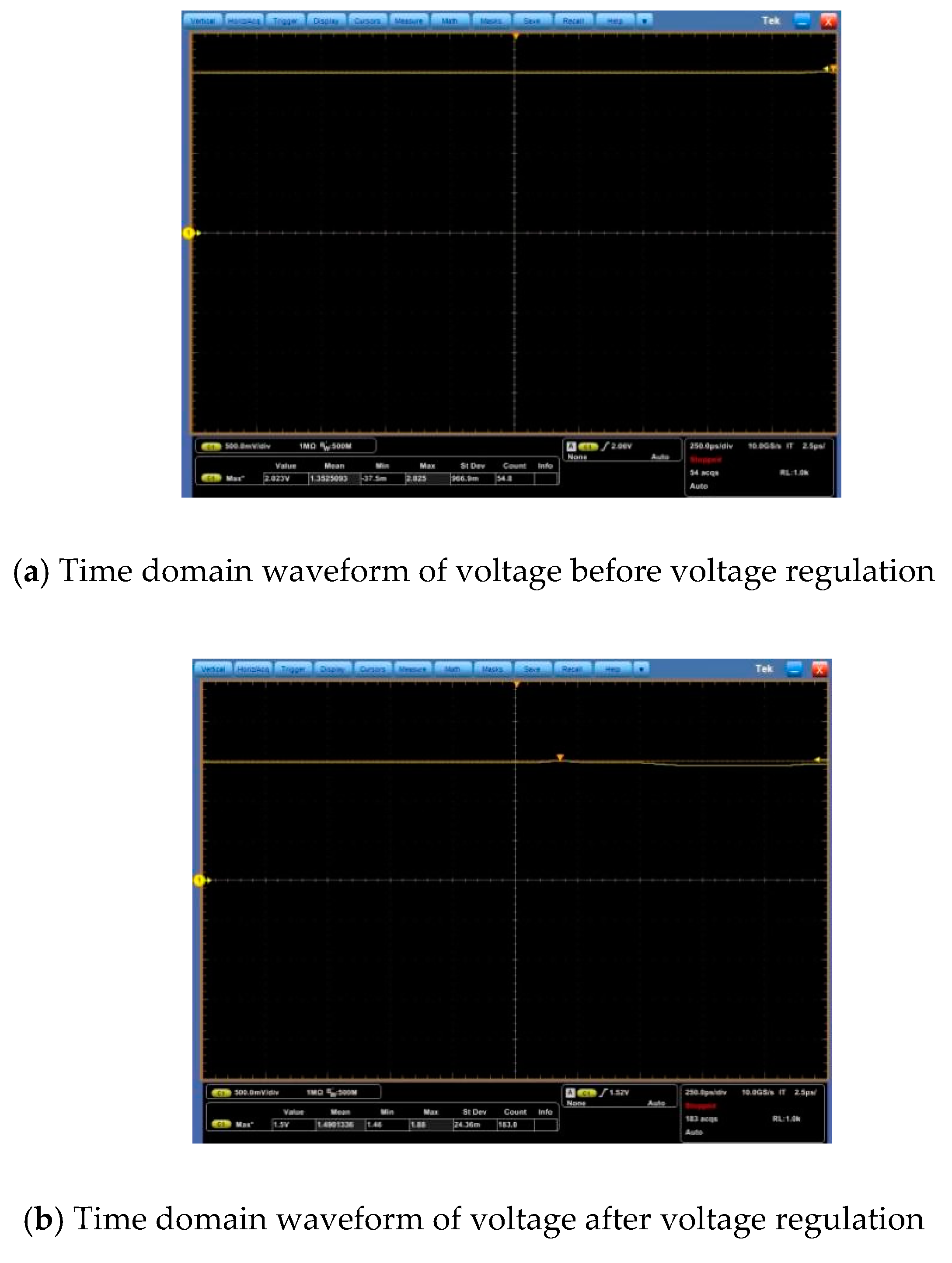
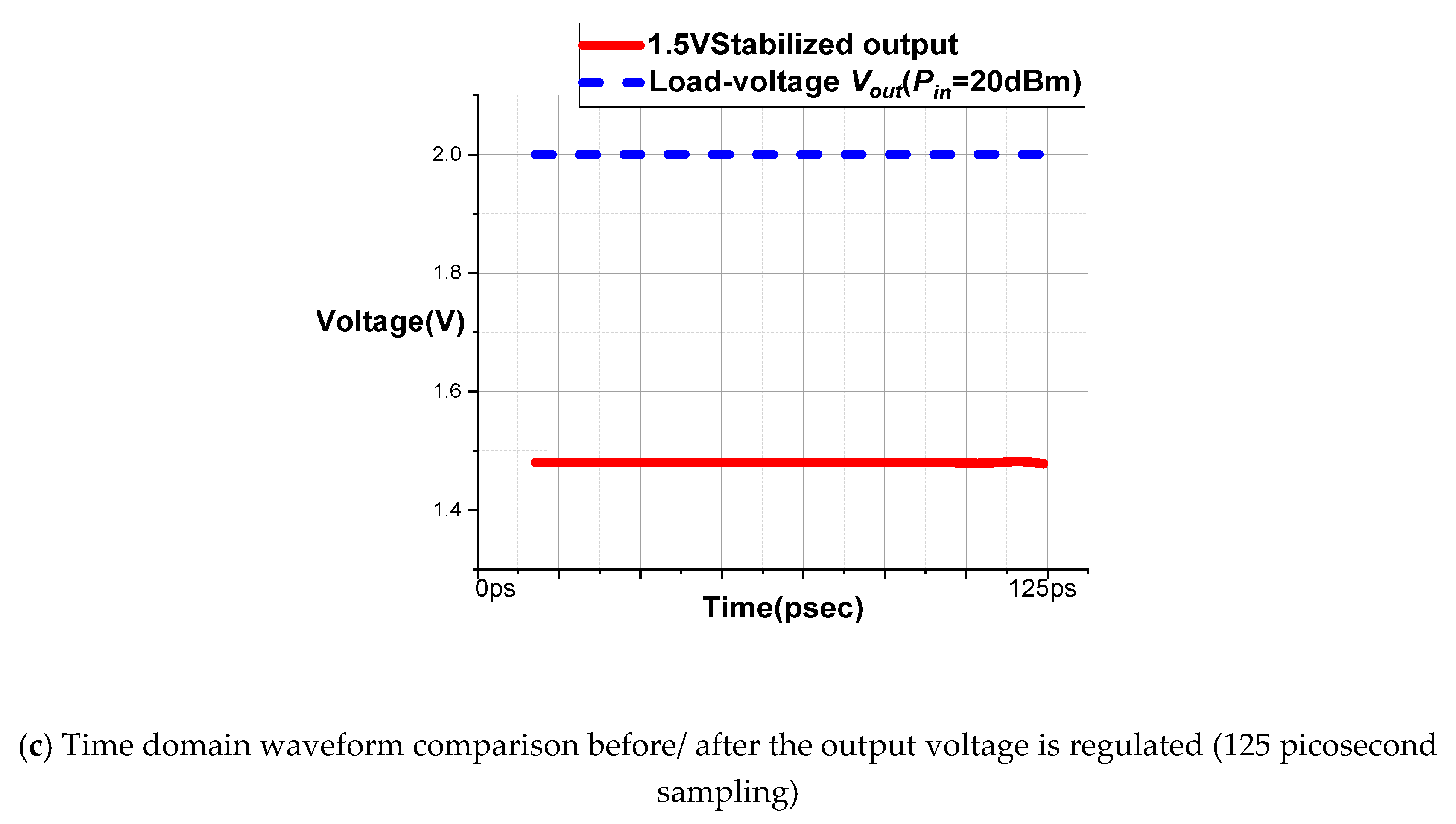
In this paper, the power of the RF generator was set to 20dBm, and the output voltage at the load side and the regulated output voltage were measured respectively, as shown in
Figure 13. When the input power
Pin = 20dBm (about 100mW) with 125 picoseconds as the sampling period to observe the output voltage situation, it could be seen in
Figure 13c that the output voltage at the load side was about 2.04V, and be stabilized around 1.5V through the regulator circuit. This indicated that the circuit had successfully implemented a four-channel microwave rectifier to convert the RF signal to DC output with an RF-DC conversion efficiency of nearly 40%.
4.2. Long-Range Wireless Charging Experiment
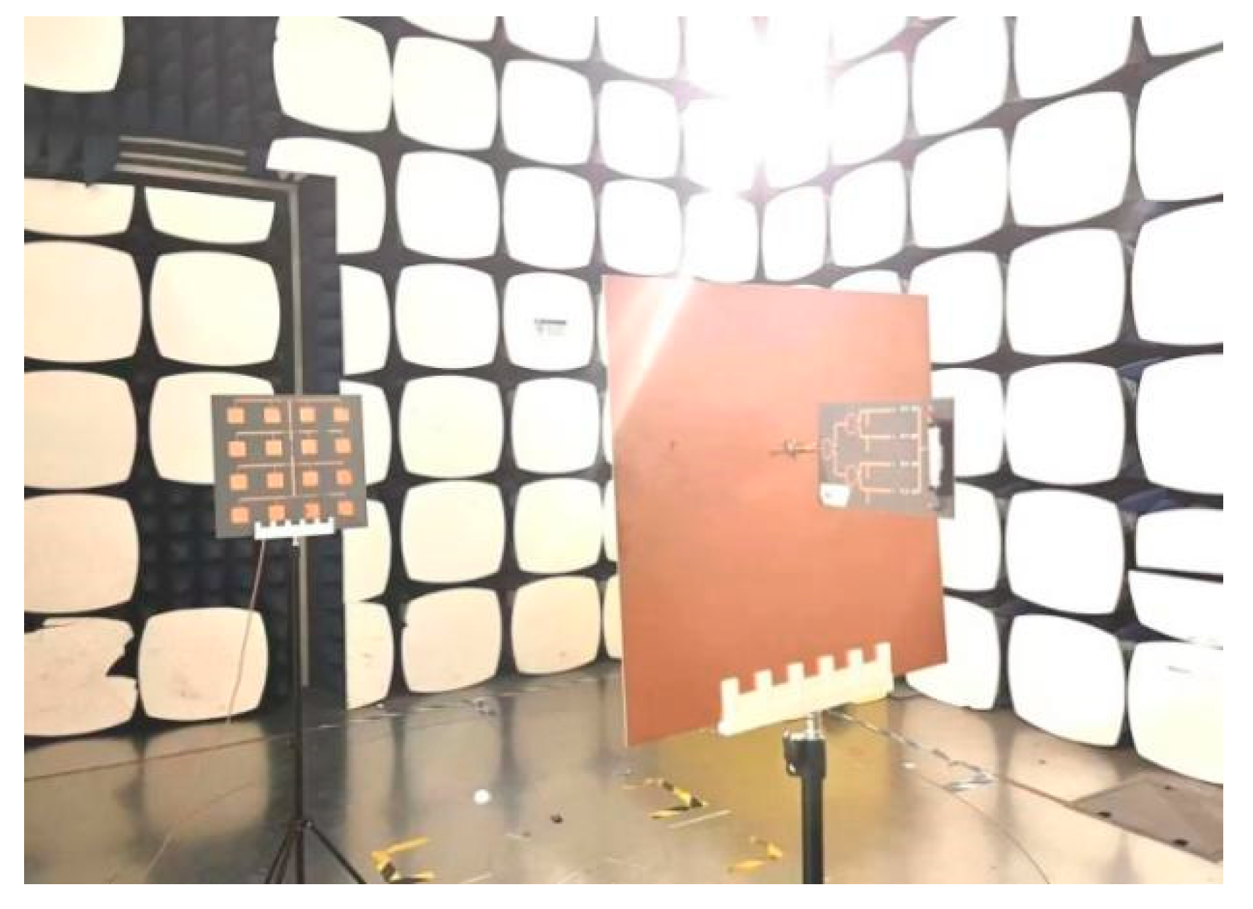
The designed four-channel microwave rectifier circuit was connected to the space transmission platform. In order to obtain better spatial transmission effect, the transmitting and receiving antennas all used 16-element circularly polarized antenna array, and were fixed by antenna brackets as well as 3D printed molded fasteners. The height of the transmitting and receiving antenna was 1.5 meters, and the distance between antennas was 3 meters. Keysight's 9310A microwave signal source was used as the RF transmitter, together with an amplifier as the microwave radiation source. The measured radiation power used in this experiment was 46dBm (about 40W) and the receiving antenna output power was 20dBm, as shown in
Figure 14.
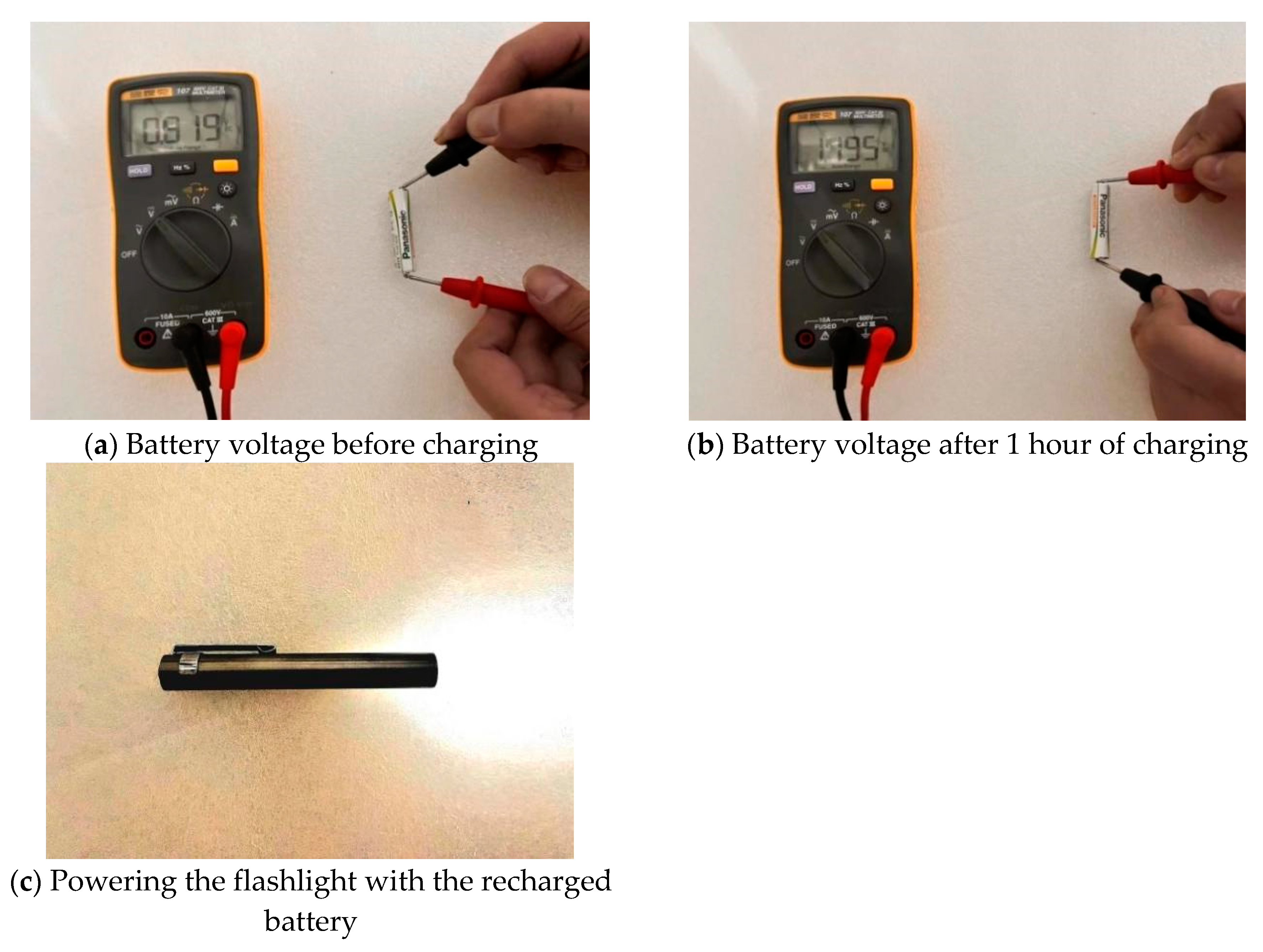
After fully discharging the Panasonic HHR-4MRC No.7 NiMH battery, it was put into the battery box of the rectifier circuit. By using the above spatial transmission scheme, the battery voltage before and after charging was measured and compared after irradiating the receiving antenna for a period of time, as shown in
Figure 15. Before charging, the battery was empty and the measured voltage was 0.82 V. After 1 hour of wireless charging, the battery power was obviously restored and the measured voltage was about 1.195 V. After about 1.5 hours, the voltage stabilized at about 1.45V, indicating that the battery had been fully charged. This proved that the MWPT system successfully completed long-range wireless charging at a distance of 3 meters, which can meet the charging requirements of some small wearable devices (e.g., cell phones, etc.) indoors.
5. Conclusions
Because the input impedance of the schottky diode to the input power is relatively sensitive, so a single channel of the rectifier circuit of power dynamic range and capacity of the power is limited, multi-path technology is often used to broaden the power dynamic range of the microwave rectifier circuit, but the rectifier channels tend to be uneven, this paper designed a model for this problem more practical microwave rectifier circuit, First each branch using the same structure, sharing one load on the output side, this design has two advantages, one is to improve the output voltage, help the weak electromagnetic energy collection, 2 it is multiple rectifier branch in DC power output can be directly synthesis, without introducing the complex power electronic transformation, which can improve the charging efficiency. This structure facilitates direct DC power synthesis at the load side. the rectifier circuit to have an RF-DC conversion efficiency greater than 50% over the input power range from 12mW to 274mW, widened by 274% compared to a single channel. A complete MWPT experimental system was built, and this rectifier circuit structure was used to achieve microwave energy collection and storage through a 16-elements CP array at a distance of 3 meters.
References
- Brown, W.C. The history of power transmission by radio waves. IEEE Trans. Microwave Theory Tech. 1984, 32, 1230–1242. [Google Scholar] [CrossRef]
- Sivagnanam, G.; Priya, P.L.; Sowmya, P.; Mathivanan, G.P. Wireless power transmission using inductive coupling. Prgramm. Dev. Circuit. Syst. 2012, 4, 260–263. [Google Scholar]
- Petersen, E.; Hansen, J.F. Self-tuning resonant power transfer systems. United States Patent 9287040.
- Cheng, S.; Chen, X.; Wang, J.; Wen, J.; Li, J. Key technologies and applications of wireless power transmission. Trans. China Electrotech. Soc. 2015, 30, 68–84. [Google Scholar] [CrossRef]
- Fan, X.; Gao, L.; Mo, X.; Zhao, Q.; Jia, E. Overview of research status and application of wireless power transmission technology. Trans. China Electrotech. Soc. 2019, 34, 1353–1380. [Google Scholar]
- Xue, F.; Liu, S.; Kong, X. Single-layer high-gain flat lens antenna based on the focusing gradient metasurface. Int. J. RF Microw. C. E. 2020, 30, e22183. [Google Scholar] [CrossRef]
- Peng, C.; Ye, Z.-H.; Xia, Y.-H.; Yang, C. Analysis on space transmission model of the Microwave Wireless Power Transfer system. Frequenz 2021, 75, 449–458. [Google Scholar] [CrossRef]
- Wang, M.; Yang, L.; Fan, Y.; Shen, M.; Li, Y.; Shi, Y. A compact omnidirectional dual-circinal rectenna for 2.45 GHz wireless power transfer. Int. J. RF Microw. C. E. 2019, 29, e21625. [Google Scholar] [CrossRef]
- Liu, Z.; Zhong, Z.; Guo, Y.-X. Enhanced dual-band ambient RF energy harvesting with ultra-wide power range. IEEE Mirow. Wirel. Co. 2015, 25, 630–632. [Google Scholar] [CrossRef]
- Niotaki, K.; Georgiadis, A.; Collado, A.; Vardakas, J.S. Dual-band resistance compression networks for improved rectifier performance. IEEE Trans. Microw. Theory 2014, 62, 3512–3521. [Google Scholar] [CrossRef]
- Zhang, X.Y.; Lin, Q.-W. High-efficiency rectifier with extended input power range based on two parallel sub-rectifying circuits. In Proceedings of the 2015 IEEE International Wireless Symposium (IWS 2015), Shenzhen, China, 30 March–1 April 2015; pp. 1–4. [Google Scholar]
- Peng, C.; Ye, Z.; Wu, J.; Chen, C.; Wang, Z. Design of a Wide-Dynamic RF-DC Rectifier Circuit Based on an Unequal Wilkinson Power Divider. Electronics 2021, 10, 2815. [Google Scholar] [CrossRef]
- Zhang, L.; Ji, S.; Gu, S.; Huang, X.; Palmer, J.E.; Giewont, W.; Wang, F.F.; Tolbert, L.M. Design considerations for high-voltage insulated gate drive power supply for 10-kV SiC MOSFET applied in medium-voltage converter. IEEE Trans. Ind. Electron. 2020, 68, 5712–5724. [Google Scholar] [CrossRef]
- Zhang, L.; Ruan, X. Control schemes for reducing second harmonic current in two-stage single-phase converter: An overview from DC-bus port-impedance characteristics. IEEE Trans. Power Electron. 2019, 34, 10341–10358. [Google Scholar] [CrossRef]
- Zhang, L.; Shi, D.; Yang, T.; Wang, K.; Tang, Y.; Loh, W.K. Split dc-bus capacitance reduction for three-phase-four-wire T-type inverter by employing power decoupling network. IEEE Trans. Ind. Electron. 2021. [Google Scholar] [CrossRef]
- Xiao, Y.Y.; Du, Z.-X.; Zhang, X.Y. High-efficiency rectifier with wide input power range based on power recycling. IEEE Trans. Circuits-II 2018, 65, 744–748. [Google Scholar] [CrossRef]
- Lin, W.; Zhao, Y.; Wen, G. Power transmission by microwave-a propulsion for modernization construction. Sci. Technol. Rev. 1994, 31–34. [Google Scholar]
- Johnson, R. Antenna engineering handbook, 2nd ed.; McGraw-Hill, Inc.: New York, NY, 1984. [Google Scholar]
- Boaventura, A.; Belo, D.; Fernandes, R.; Collado, A.; Georgiadis, A.; Carvalho, N.B. Boosting the efficiency: Unconventional waveform design for efficient wireless power transfer. IEEE Microw. Mag. 2015, 16, 87–96. [Google Scholar] [CrossRef]
|
Disclaimer/Publisher’s Note: The statements, opinions and data contained in all publications are solely those of the individual author(s) and contributor(s) and not of MDPI and/or the editor(s). MDPI and/or the editor(s) disclaim responsibility for any injury to people or property resulting from any ideas, methods, instructions or products referred to in the content. |
© 2023 by the authors. Licensee MDPI, Basel, Switzerland. This article is an open access article distributed under the terms and conditions of the Creative Commons Attribution (CC BY) license (http://creativecommons.org/licenses/by/4.0/).
