Submitted:
25 May 2023
Posted:
26 May 2023
You are already at the latest version
Abstract
This work reports the first nanocrystalline SnON (7.6 % Nitrogen content) n-type nanosheet Field-Effect Transistor (nFET) with transistor’s effective mobility (µeff) as high as 357 and 325 cm2/V-s at electron density (Qe) of 5×1012 cm-2 and ultra-thin body thickness (Tbody) of 7 and 5 nm, respectively. At the same Tbody and Qe, these µeff values are significantly higher than single crystalline Si, InGaAs, thin-body Si-on-Insulator (SOI), two-dimensional (2D) MoS2 and WS2. New discovery of slower µeff decay rate at high Qe than SiO2/bulk-Si universal curve was found, owing to one order of magnitude lower effective field (Eeff) by more than 10 times higher dielectric constant () in channel material, which keeps the electron wave-function away from the gate-oxide/semiconductor interface and lowers the gate-oxide surface scattering. In addition, the high µeff is also due to the overlapped large radius s-orbitals, low 0.29 mo effective mass (me*) and low polar optical phonon scattering. SnON nFETs with record-breaking µeff and quasi-2D thickness enable potential monolithic three-dimensional (3D) integrated circuit (IC) and embedded memory for 3D biological brain-mimicking structures.
Keywords:
high mobility
; thin film transistors
; SnON
; SnO2
; density functional theory
1. Introduction
Modern processors, with over 100 billion transistors, are among the most complex systems. To meet the ever-changing demand for small and high-performance devices, processor transistor density and performance must be increased. Therefore, Moore's law must be preserved, i.e., transistor must be kept shrinking in size. Fin Field Effect Transistor (FinFET) technology is a game changer in enabling 22 to 3 nm technology nodes [1,2]. However, at sub-3 nm technology nodes in the near future, FinFET technology will face critical challenges of limited area scaling and performance degradation. The Fin width can no longer be scaled down due to increased threshold voltage (Vth) shift and lowered transistor’s effective mobility (μeff) [3]. Gate length is also difficult to reduce due to transistor’s quantum-mechanical (QM) tunneling from source to drain [4], resulting in high leakage current even when the transistor is off. Nanosheet (NS) transistors are the best solution to overcome these challenges of FinFET scaling, enabling higher drive currents [5,6]. NS-FETs are suitable for high computing needs due to their compatibility with various materials such as InGaAs, two-dimensional (2D) MoS2 and WS2, among others.
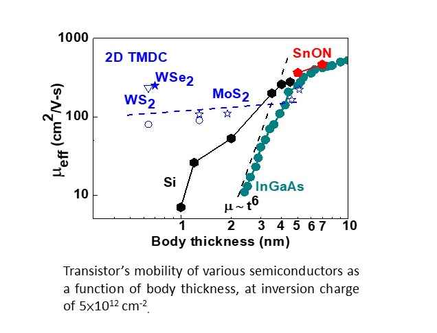
The downscaling of Si NS complementary FET is planned to 1 nm node, but further shrinking device is limited by the 2D material and hyper numerical-aperture (NA) extreme-ultraviolet (EUV) lithography. Unfortunately, there is no known solution to form defect-free and uniform monolayer 2D material over the 12-inch wafer. The rapidly increasing cost and huge power consumption are the major bottlenecks to realize hyper-EUV lithography system. Those downscaling barriers may be overcome by the monolithic three-dimensional (3D) structure [4,7,8] that mimic the bio-brain. In addition, monolithic 3D integrated circuits (ICs) can provide better performance of higher operating frequencies and lower power consumption than their 2D counterparts [7]. Yet the poor µeff for transistor made on backend dielectric of an IC is the basic challenge. Peviously, we reported high field-effect mobility (µFE) of SnO2 [4,9,10] and SnON FET [11], but the effective mobility (µeff) is the required important data for transistors. The µeff can give crucial information on electron scattering mechanisms over the wide range of inversion charge (Qe). The Qe or gate voltage (VG) dependent µeff is also essential for device modeling used for IC design. In this report, we measure the transistor output current over a wide range of VG, equivalent to a Qe close to 1×1013 cm-2, to analyze the device scaling mechanism. Such high Qe is critical to deliver a high transistor’s output current and drive the IC speed quickly. The µeff degrades monotonically with increasing charge density is the physical limitation of a Metal-Oxide-Semiconductor FET (MOSFET). However, the MOSFET must be biased at high charge density to deliver a high output current. For the first time, this fundamental restriction is overcome by using a higher dielectric constant (κ) and high µeff channel. The nanocrystalline SnON n-type FET (nFET) has µeff as high as 325 cm2/V-s at 5×1012 cm-2 electron density (Qe) and 5 nm nanosheet body thickness (Tbody). At the same Tbody, this µeff is significantly higher than single-crystalline Si, InGaAs, 2D MoS2, 2D WS2 and 2D WSe2. The high µeff is also due to small 0.29 mo effective mass (me*), overlapped large radius s-orbital, signifincatly lower effective field (Eeff) by >10× higher κ value than Si, GaAs, InP, GaN and SiC. The N3- anions having higher p orbital energy can move up valance band (EV) from first principle QM calculation and the Oxygen vacancy levels (Vo) residing in the channel layer are reduced to improve the µeff. The 3D 400oC process of SnON does not require a single crystal substrate; thus, the energy consumption is many orders of magnitude lower than today's single crystal Si wafer. The record-high µeff and quasi-2D thickness SnON nFET suggest potential monolithic three-dimensional (3D) and embedded dynamic random access memory (DRAM), to mimic the 3D bio-brain structure.
2. Materials and Methods
The bottom-metal-gate/high-κ/[SnON or SnO2] nFETs were made by depositing a 50 nm TaN as bottom gate using reactive sputtering. Then, a 45-nm high-κ HfO2 and 3-nm SiO2 were deposited as a gate dielectric using electron-beam evaporator and annealed at 400°C under oxygen environment for 30 minutes using furnace. Further, SnON or SnO2 channel layer were deposited by reactive sputtering using Sn target (purity 99.99%) followed by post-annealing at 400oC. The Sn sputter power, argon flow rate and process pressure is fixed at 30 W, 24 sccm and 7.6 × 10⁻³ torr respectively. O2 flow rate is fixed at 20 sccm for SnO2 channel layer. 7.6 % Nitrogen content (30 sccm of Nitrogen) are used for deposition of SnON channel layer. The source-drain electrodes of 80 nm thick Al was deposited and patterned using thermal coater. The fabricated nFET has channel length of 50 μm and width of 500 μm, respectively. The material properties of SnON and SnO2 were studied using first principle QM calculations [12]. The Broyden-Fletcher-Goldfarb-Shanno (BFGS) minimization technique has been used to optimize the crystal structure [13]. It was done using the self-consistent field approach, which has a convergence precision of 1×10⁻⁸ eV/atom. This study made use of the generalized gradient approximation (GGA) with local density approximation plus U (LDA+U) approach. The energy cutoff for enlarging the plane wave basis set was set at 430 eV, and the Brillouin zone was sampled using the Monkhorst-Pack k-point approach with the k-points (6 ×6×5) [14].
3. Results
Using first principle calculations based on density functional theory, the density of state (DOS) for SnO2 and SnON were examined as shown in Figure 1 (a) and (b), respectively. For convenience of analysis, the valence band maximum (VBM) was adjusted to zero. The lower conduction states close to the conduction band minimum (CBM) in SnO2 and SnON were primarily produced from Sn 5s orbitals [15], while the localized states immediately above the VBM in SnON had a predominance of N 2p character. The N states in the valence band, principally N 2p character, are the main cause of the bandgap reduction in SnON. SnO2 and N2 doped SnO2 have effective electron masses (me*) of 0.41 mo and 0.29 mo, respectively, where mo is the free electron mass which is reported in our previous work [11]. The me* for SnON is evidently smaller than SnO2, which could result in a larger µeff.
Figure 2 (a)-(c) depicts the transistor’s drain-current versus drain-voltage (ID-VD) characteristics at various VG for SnO2 and SnON nFETs with Tbody of 5 nm and 7 nm. A clear pinch-off and good current saturation were measured. The SnON nFETs displayed higher ID compared to control SnO2 device. Because the metal-gate/high-κ was made at the same run with identical gate oxide capacitance, the only reason to cause significantly higher ID at the same VG-VT of SnON nFET is due to the higher µeff.
Figure 3 (a) and (b) display gate-current versus gate-voltage (IG-VG) and ID-VG transfer characteristics at a VD=0.1 V for SnON nFETs with Tbody of 5 and 7 nm. Large on-current/off-current (ION/IOFF) is achieved in 5 nm Tbody thickness that is important for IC application. The FET’s scattering mechanism is further analyzed by the µeff as a function of Qe. As shown in Figure 3 (c), at low to medium Qe, the nFET’s µeff of SnO2 is significantly lower than SnON one. The SnO2 nFET shows much faster µeff degradation with increasing Qe. Although the oxide charges in high-κ dielectric is responsible for lower µeff than conventional SiO2 gate dielectric [16,17,18,19], such µeff reduction is most significant at high Qe rather than at low Qe. It is reported that the µeff at low Eeff or Qe is due to coulomb scattering from charged impurities [20]. The potential reason for such larger µeff of SnON nFET than that of SnO2 may be related to the lower charged Vo. By injecting non-oxide nitrogen anions, SnON can lower the defect trap densities. This allows for the removal or passivation of Vo through substitutional alloying with N3- to improve the μeff as seen in Figure 4. Similar observations were also found with ZnON [21]. It is well-known that the transition SiOx between Si and SiO2 gives a positive fixed oxide charge, primarily due to structural Vo defects in the oxide layer. Such positive Vo charge close to valence band in SnON may be lowered by extra N-band as shown in DOS of Figure 1(b).
Figure 5 (a) further plots 1/µeff vs. Qe, and the large slope in the low Qe is related to charged Vo scattering in SnO2 that is lowered by adding N3- anions. We further compare the µeff-Qe dependence for universal SiO2/bulk-Si, SiO2/Si-on-Insulator (SOI), high-κ/SnO2, and high-κ/SnON nFETs. As shown in Figure 5 (b), the µeff as high as 357 and 325 cm2/V-s are achieved at Qe of 5×1012 cm-2 and Tbody of 7 and 5 nm, respectively. At 1×1013 cm-2 Qe, an ultra-thin 5 and 7 nm thickness, the µeff of high-κ/SnON nFET is 85% and 95% of universal SiO2/bulk-Si nFET. The µeff scattering mechanism of SiO2/bulk-Si nFET at low, medium, and high Eeff is due to coulomb, phonon, and surface scattering, respectively. The universal µeff of SiO2/bulk-Si nFET depends on standard Qe-0.3 in medium Qe, which becomes Qe-0.6 dependence at high Qe to 1×1013 cm-2. However, the µeff decay rate of high-κ/SnO2 and high-κ/SnON nFETs at high Qe is much slower than universal SiO2/bulk-Si and thin-body SOI nFETs [22]. To understand such abnormal slow μeff dependence on Qe, we further measured the dielectric constant, κ of 5 nm SnO2. Figure 6 shows the measured capacitance under various voltage at 1 kHz. The SnO2 has a κ of 123 that is >10× larger than major semiconductors of Si, GaAs, InP, GaN, SiC etc [23,24,25,26,27]. This high κ value is also close to the reported data in literature [28]. The novel discovery μeff dependence on Qe-0.30 at high Qe range is due to the >10× higher κ value to keep high-κ/SnON nFET at medium Eeff range. Here the Eeff is proportional to Qe:
The εsemi equals ε0κ, where εsemi and ε0 are permittivity of semiconductor and free space respectively. Ndep is the depletion charge of charged impurities in doped Si or charged Vo in major oxide semiconductors. The n factor in SiO2/bulk-Si equals to 2 and 3 for nMOSFET and pMOSFET, respectively. The significantly much higher κ value than most of the commercial semiconductors of Si, GaAs, InP, GaN and SiC allow the channel electrons to keep a low Eeff. This in turn keeps the electron wave-functions in the conduction channel [29] away from the gate-oxide/semiconductor interface and decreases the gate-oxide surface scattering.
It is important to notice that the μeff of SnON nFET are the highest values among all the oxide-based semiconductors. This is due to the smaller me* and larger phonon energy (Eop) [30] to give high μeff:
The total μeff can be expressed as:
Here the µVo is the FET’s mobility that is limited by charged Vo. This µVo is extremely important at low to medium Qe shown in Figure 3 (c). The radius of s-orbital increases with increasing principle quantum number n with n2 dependence, so the overlapping s-orbitals are stronger for SnO2 than ZnO [15]. This explains why the mobility of SnON nFET is significantly larger than that of ZnO.
Table 1 compares device performance. The wide energy bandgap (EG) nanocrystalline SnON nFET has the highest µeff among single crystal Si, InGaAs, 2D MoS2, and 2D WS2. It is noticed that the next 2 nm node commercial NS nFET will use single crystalline Si with a Tbody of 7 nm, since the µeff decreases with decreasing Tbody with a Tbody6 dependence [3]. The µeff of high-κ/SnON nFETs is 2.7 times higher than that of Si nFET at the same 5 nm Tbody, which could be used for downscaling the NS Tbody. The wide-EG SnON also leads to large ION/IOFF as shown in Figure 3 (a).
4. Conclusions
In this work, we demonstrated record high µeff 5-nm Tbody nFETs, made on IC’s backend for monolithic 3D usage. For the first time, the µeff of 325 cm2/V-s at 5×1012 cm-2 Qe is 2.7 times higher than that of Si nFET at the same Tbody of 5 nm. This was achieved using wide-EG 5 nm quasi-2D SnON channel at 400oC process. Such high FET’s µeff is due to the smaller 0.29 mo, overlapped large-radius s-orbitals, and low polar optical phonon scattering. In addition, smaller µeff decay rate than SiO2/bulk-Si nFET at high Qe was found, owing to <10× Eeff by >10× higher κ value. Record high µeff SnON nFETs formed on IC's backend is the empowering technology for monolithic 3D ICs.
Author Contributions
Pheiroijam Pooja did the simulation and writing, Chun Che Chien did the experiments; Albert Chin is the principal investigator (PI) to monitor the project. All authors reviewed the manuscript.
Funding
This research was funded by National Science and Technology Council of Taiwan, project no. 110-2221-E-A49-137-MY3.
Data Availability Statement
The data presented in this study are available on request from the corresponding author. The data are not publicly available due to privacy
Acknowledgments
We would like to thank the National Yang Ming Chiao Tung university nano facility center for providing the laboratory instruments.
Conflicts of Interest
The authors declare no conflict of interest.
References
- Loubet, N.; Hook, T.; Montanini, P.; Yeung, C.W.; Kanakasabapathy, S.; Guillom, M.; Yamashita, T.; Zhang, J.; Miao, X.; Wang, J.; Young, A. Stacked nanosheet gate-all-around transistor to enable scaling beyond FinFET. In IEEE Symposium on VLSI Technology, Kyoto, Japan; 2017; pp. 230–231.
- Jang, D.; Yakimets, D.; Eneman, G.; Schuddinck, P.; Bardon, M.G.; Raghavan, P.; Spessot, A.; Verkest, D.; Mocuta, A. Device exploration of nanosheet transistors for sub-7-nm technology node. IEEE Trans. Electron Dev. 2017, 64, 2707–2713. [Google Scholar] [CrossRef]
- Low, T.; Li, M.F.; Fan, W.J.; Ng, S.T.; Yeo, Y.C.; Zhu, C.; Chin, A.; Chan, L.; Kwong, D.L. Impact of surface roughness on silicon and germanium ultra-thin-body MOSFETs, In IEDM Technical Digest. IEEE International Electron Devices Meeting, 2004; San Francisco, CA, USA; pp. 151–154. [Google Scholar]
- Shih, C.W.; Chin, A.; Lu, C.F.; Yi, S.H. Extremely high mobility ultra-thin metal-oxide with ns2np2 configuration, In IEDM Technical Digest. IEEE International Electron Devices Meeting, Washington, DC, USA, 2015; pp. 145–148. [Google Scholar]
- Liu, Y.; Duan, X.; Huang, Y.; Duan, X. Two-dimensional transistors beyond graphene and TMDCs, Chem. Soc. Rev. 2018, 47, 6388–6409. [Google Scholar] [CrossRef] [PubMed]
- Kim, J.; Lee, J.S.; Han, J.W.; Meyyappan, M. Single-event transient in FinFETs and nanosheet FETs. IEEE Electron Device Lett. 2018, 39, 1840–1843. [Google Scholar] [CrossRef]
- Yu, D.S.; Chin, A.; Laio, C.C.; Lee, C.F.; Cheng, C.F.; Chen, W.J.; Zhu, C.; Li, M.-F.; McAlister, S.P.; Kwong, D.L. 3D GOI CMOSFETs with Novel IrO2(Hf) dual gates and high-κ dielectric on 1P6M-0.18μm-CMOS. In IEDM Technical Digest. IEEE International Electron Devices Meeting, San Francisco, CA, USA; 2004; pp. 181–184. [Google Scholar]
- Chin, A.; Chen, Y.D. Technologies Toward Three-Dimensional Brain-Mimicking IC Architecture. In EDTM Technical Digest. IEEE Electron Devices Technology & Manufacturing Conference, Singapore; 2019; pp. 472–474. [Google Scholar]
- Yen, T.J.; Chin, A.; Gritsenko, V. High-performance top-gate thin-film transistor with an ultra-thin channel layer. Nanomaterials 2020, 10, 2145. [Google Scholar] [CrossRef] [PubMed]
- Shih, C.W. ; Chin; A., Lu, C.F.; Su, W.F. Low-temperature processed tin oxide transistor with ultraviolet irradiation. IEEE Electron Device Lett. 2019, 40, 909–912. [Google Scholar] [CrossRef]
- Pooja, P.; Che, C.C.; Zeng, S.H.; Lee, Y.C.; Yen, T.J.; Chin, A. Outstanding High Field-Effect Mobility of 299 cm2V−1s−1 by Nitrogen-Doped SnO2 Nanosheet Thin-Film Transistor, Adv. Mater. Technol. 2023, 2201521. [Google Scholar]
- Bussolotti, F.; Yang, J.; Kawai, H.; Chee, J.Y.; Goh, K.E.J. Influence of many-body effects on hole quasiparticle dynamics in a WS2 monolayer, Phys. Rev. B 2021, 103, 045412. [Google Scholar] [CrossRef]
- Fischer, T.H.; Almlof, J. General methods for geometry and wave function optimization. The J. Phys. Chem. 1992, 96, 9768–9774. [Google Scholar] [CrossRef]
- Monkhorst, H.J.; Pack, J.D. Special points for Brillouin-zone integrations. Phys. Rev. B 1976, 13, 5188. [Google Scholar] [CrossRef]
- Shih, C.W.; Chin, A.; Lu, C.F.; Su, W.F. Remarkably high hole mobility metal-oxide thin-film transistors. Sci. Rep. 2016, 6, 19023. [Google Scholar] [CrossRef]
- X. Yu, C. X. Yu, C. Zhu, M. Yu, M.F. Li, Albert Chin, C.H. Tung, D. Gui, and D. L. Kwong, “Advanced MOSFETs using HfTaON/SiO2 Gate Dielectric and TaN Metal Gate with Excellent Performance for Advanced Low Standby Power Application,” IEEE International Electron Devices Meeting (IEDM) Tech. Dig. Washington DC, Dec. 2005; pp. 31–34. [Google Scholar]
- D. S. Yu, Albert Chin, C.H. Wu, M.-F. Li, C. Zhu, S.J. Wang, W.J. Yoo, B.F. Hung and S. P. McAlister, “Lanthanide and Ir-based Dual Metal-Gate/HfAlON CMOS with Large Work-Function Difference,” IEEE International Electron Devices Meeting (IEDM) Tech. Dig. Washington DC, Dec. 2005; pp. 649–652.
- C. H. Wu, B.F. Hung, Albert Chin, S.J. Wang, X.P. Wang, M.-F. Li, C. Zhu, Y. Jin, H.J. Tao, S.C. Chen, and M. S. Liang “High Temperature Stable [Ir3Si-TaN]/HfLaON CMOS with Large Work-Function Difference,”. IEEE International Electron Devices Meeting (IEDM) Tech. Dig., San Francisco, CA, Dec. 2006; pp. 617–620.
- C. F. Cheng, C.H. Wu, N.C. Su, S.J. Wang, S.P. McAlister and Albert Chin, “Very Low Vt [Ir-Hf]/HfLaO CMOS Using Novel Self-Aligned Low Temperature Shallow Junctions". In IEEE International Electron Devices Meeting (IEDM) Tech. Dig., Washington DC; Dec. 2007; pp. 333–336.
- Takagi, S.I.; Toriumi, A.; Iwase, M.; Tango, H. On the universality of inversion layer mobility in Si MOSFET's: Part I-effects of substrate impurity concentration. IEEE Trans. on Electron Dev. 1994, 41, 2357–2362. [Google Scholar] [CrossRef]
- Park, J.; Jeong, H.J.; Lee, H.M.; Nahm, H.H.; Park, J.S. The resonant interaction between anions or vacancies in ZnON semiconductors and their effects on thin film device properties. Sci. Rep. 2017, 7, 2111. [Google Scholar] [CrossRef] [PubMed]
- Rim, K.; Chan, K.; Shi, L.; Boyd, D.; Ott, J.; Klymko, N.; Cardone, F.; Tai, L.; Koester, S.; Cobb, M.; Canaperi, D. Fabrication and mobility characteristics of ultra-thin strained Si directly on insulator (SSDOI) MOSFETs. In IEDM Technical Digest. IEEE International Electron Devices Meeting, Washington, DC, USA, 2003; pp. 1–4. [Google Scholar]
- Baroni, S.; Resta, R. Ab initio calculation of the macroscopic dielectric constant in silicon. Phys. Rev. B 1986, 33, 7017. [Google Scholar] [CrossRef] [PubMed]
- Kunc, K.; Resta, R. External fields in the self-consistent theory of electronic states: a new method for direct evaluation of macroscopic and microscopic dielectric response. Phys. Rev.Lett. 1983, 51, 686. [Google Scholar] [CrossRef]
- Neidert, R.E.; Binari, S.C.; Weng, T. Dielectric constant of semi-insulating indium phosphide. Electronic. Lett. 1982, 18, 987–988. [Google Scholar] [CrossRef]
- Kane, M.J.; Uren, M.J.; Wallis, D.J.; Wright, P.J.; Soley, D.E.J.; Simons, A.J.; Martin, T. Determination of the dielectric constant of GaN in the kHz frequency range. Semicond. Sci. Technol. 2011, 26, 085006. [Google Scholar] [CrossRef]
- Moore, W.J.; Holm, R.T.; Yang, M.J.; Freitas Jr, J.A. Infrared dielectric constant of cubic SiC. J. Appl. Phys. 1995, 78, 7255–7258. [Google Scholar] [CrossRef]
- Youssef, A.M.; Yakout, S.M. Colossal dielectric constant, electric modulus and electrical conductivity of nanocrystalline SnO2: Role of Zr/Mn, Fe or Co dopants. J. Solid State Chem 2022, 308, 122902. [Google Scholar] [CrossRef]
- Yi, S.H.; Ruan, D.B.; Di, S.; Liu, X.; Wu, Y.H.; Chin, A. High performance metal-gate/high-k GaN MOSFET With good reliability for both logic and power applications. IEEE J. Electron Devices Soc. 2016, 4, 246–252. [Google Scholar] [CrossRef]
- Shih, C.W.; Chin, A. New material transistor with record-high field-effect mobility among wide-band-gap semiconductors. ACS Appl. Mater. Interfaces 2016, 8, 19187–19191. [Google Scholar] [CrossRef]
- Shan, W.; Walukiewicz, W.; Ager, J.W.; Yu, K.M.; Yuan, H.B.; Xin, H.P.; Cantwell, G.; Song, J.J. Nature of room-temperature photoluminescence in ZnO. Appl. Phys. Lett. 2005, 86, 191911. [Google Scholar] [CrossRef]
- Jarzebski, Z.M.; Morton, J.P. Physical properties of SnO2 materials: III. Optical properties. J. Electrochem. Soc. 1976, 123, 333C. [Google Scholar] [CrossRef]
- Ogino, T.; Aoki, M. Photoluminescenece in P-doped GaN. Jpn. J. App. Phys. 1979, 18, 1049. [Google Scholar] [CrossRef]
- Minamitani, E.; Arafune, R.; Frederiksen, T.; Suzuki, T.; Shahed, S.M.F.; Kobayashi, T.; Endo, N.; Fukidome, H.; Watanabe, S.; Komeda, T. Atomic-scale characterization of the interfacial phonon in graphene/SiC. Phys. Rev. B. 2017, 96, 155431. [Google Scholar] [CrossRef]
Figure 1.
(a) DOS of Sn in SnO2 and (b) DOS of N in SnON calculated using first principle density functional theory.
Figure 1.
(a) DOS of Sn in SnO2 and (b) DOS of N in SnON calculated using first principle density functional theory.
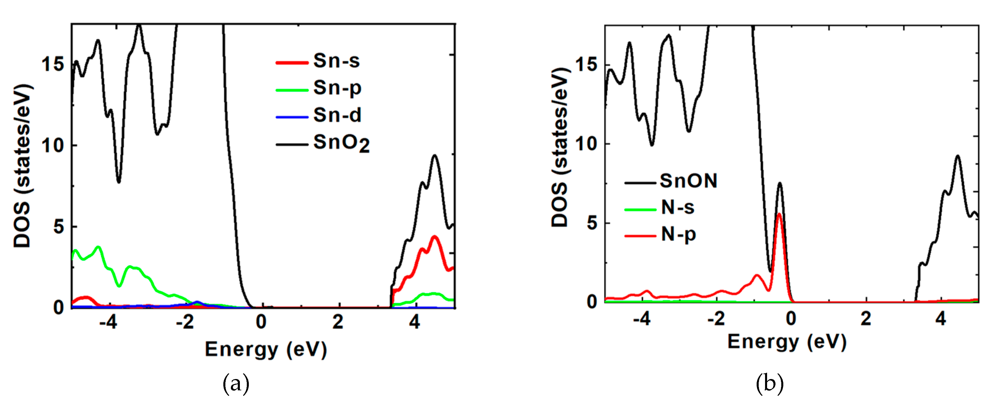
Figure 2.
ID-VD output characteristics for (a) TaN/HfO2/5-nm-SnO2 nFET (b) TaN/HfO2/5-nm-SnON nFET and (c) TaN/HfO2/7-nm-SnON nFET.
Figure 2.
ID-VD output characteristics for (a) TaN/HfO2/5-nm-SnO2 nFET (b) TaN/HfO2/5-nm-SnON nFET and (c) TaN/HfO2/7-nm-SnON nFET.
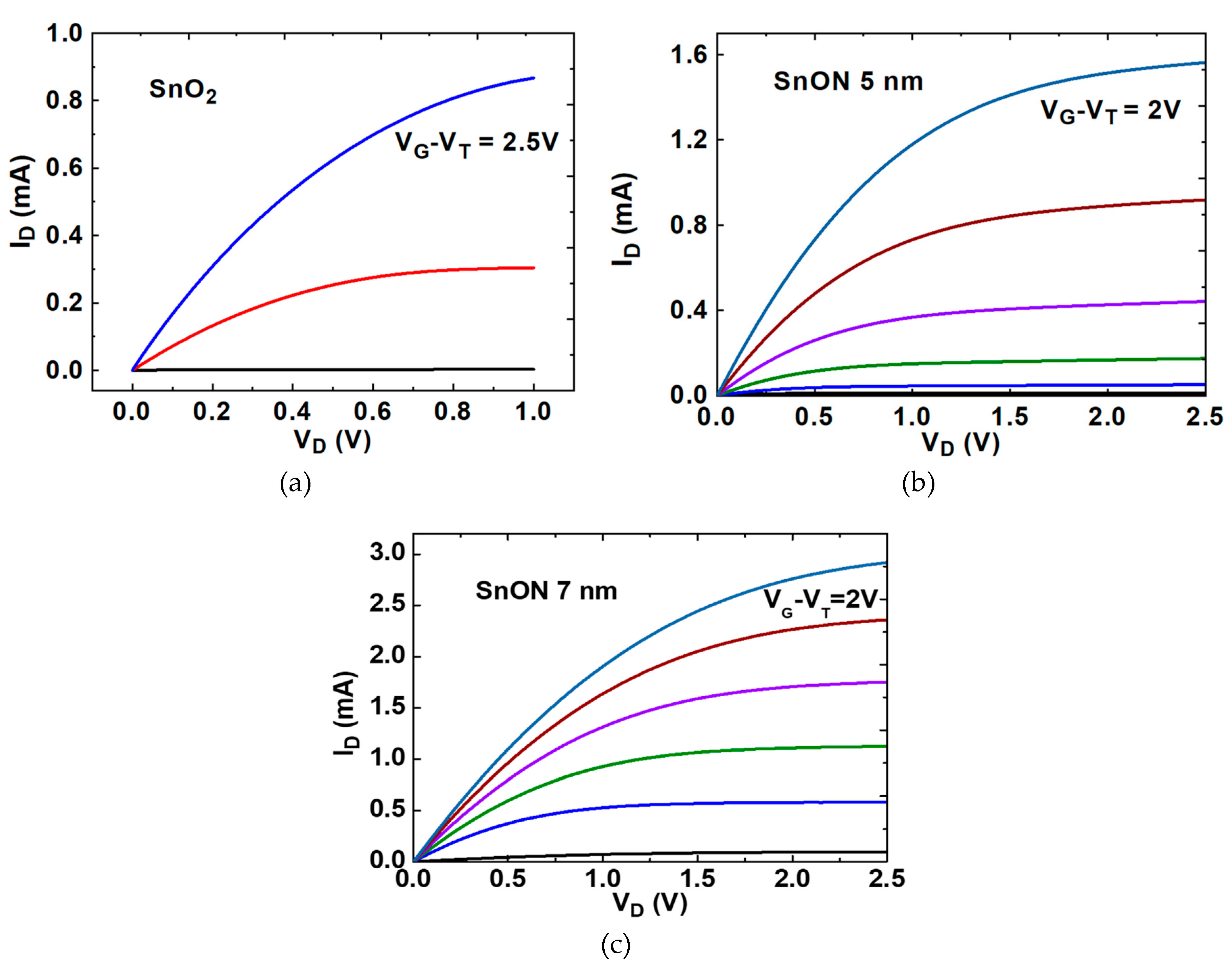
Figure 3.
IG-VG and ID-VG transfer characteristics for (a) TaN/HfO2/5-nm-SnON nFET and (b) TaN/HfO2/7-nm-SnON nFET; and (c) μeff versus Qe for 5-nm SnO2 and SnON nFETs.
Figure 3.
IG-VG and ID-VG transfer characteristics for (a) TaN/HfO2/5-nm-SnON nFET and (b) TaN/HfO2/7-nm-SnON nFET; and (c) μeff versus Qe for 5-nm SnO2 and SnON nFETs.
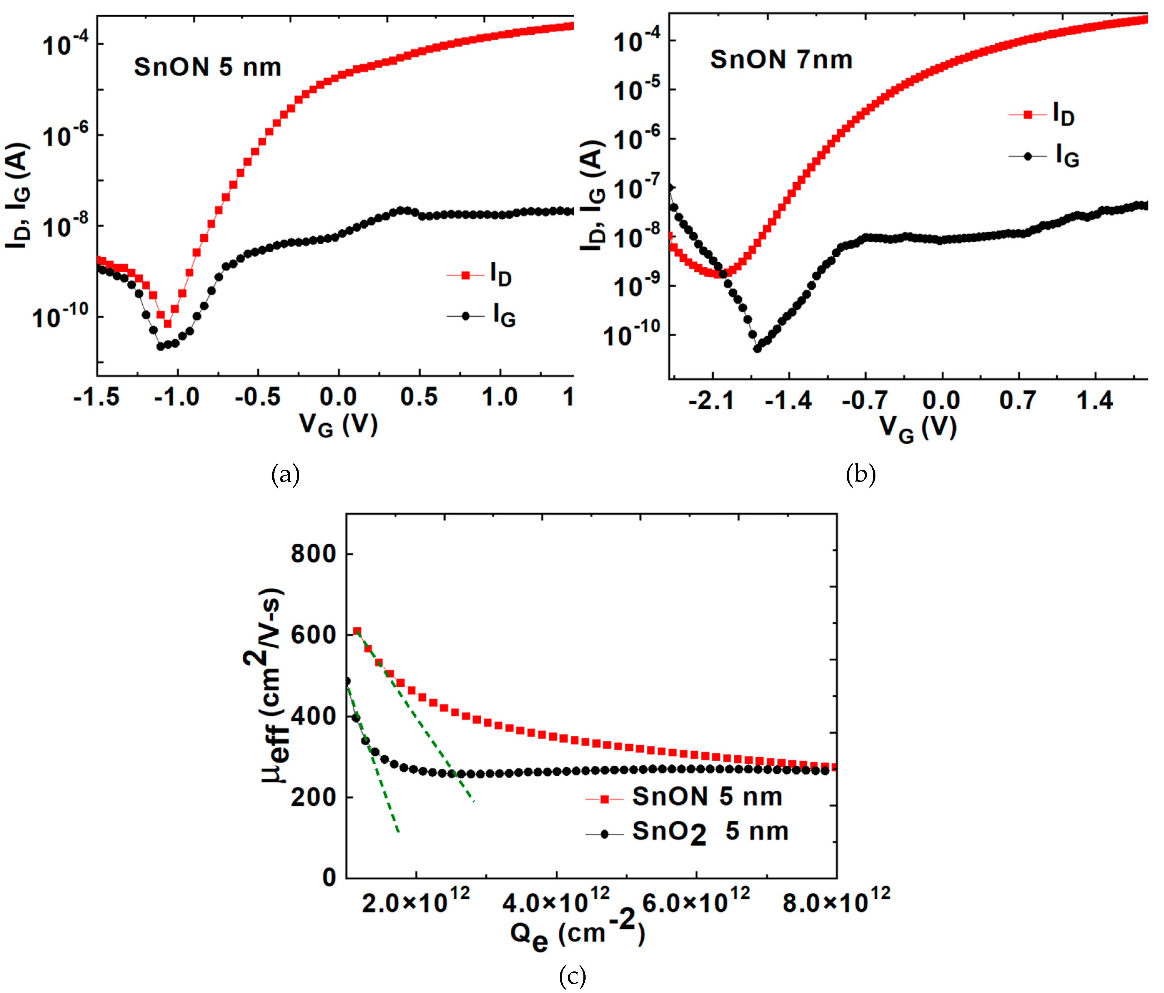
Figure 4.
Diagrammatic sketch of substitutional alloying of Oxygen vacancy with Nitrogen atom
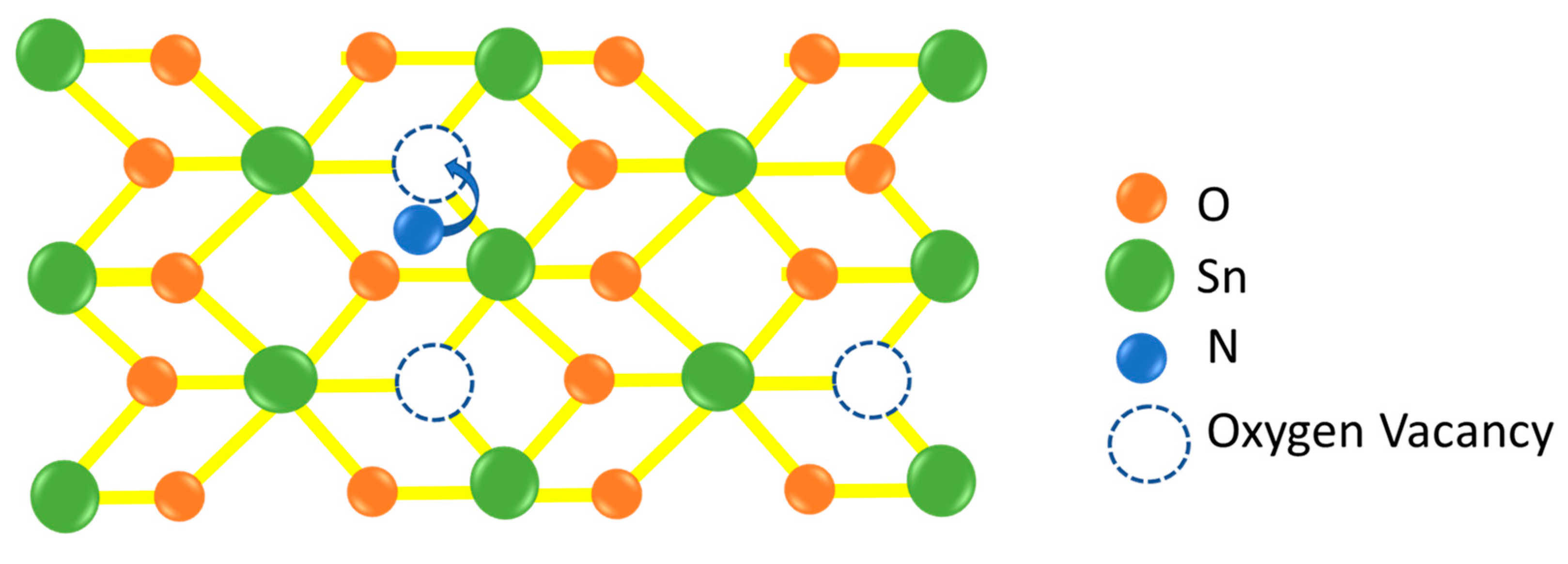
Figure 5.
(a) 1/μeff versus Qe plot for 5-nm SnO2, 5-nm SnON and 7-nm SnON nTFTs and (b) μeff versus Qe with different channel thickness of SnON nFET and comparison with SOI [22] and universal nFETs.
Figure 5.
(a) 1/μeff versus Qe plot for 5-nm SnO2, 5-nm SnON and 7-nm SnON nTFTs and (b) μeff versus Qe with different channel thickness of SnON nFET and comparison with SOI [22] and universal nFETs.
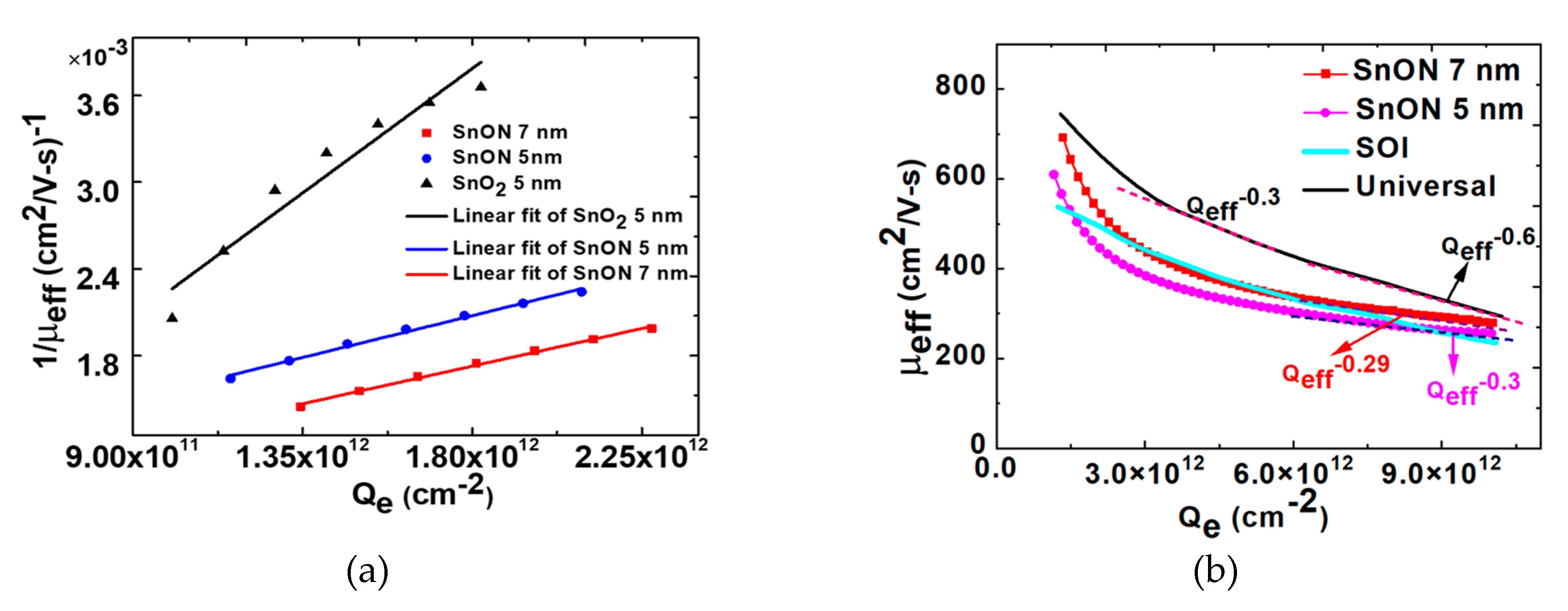
Figure 6.
C-V and I-V plot for Ni/SnO2/Ni capacitor.
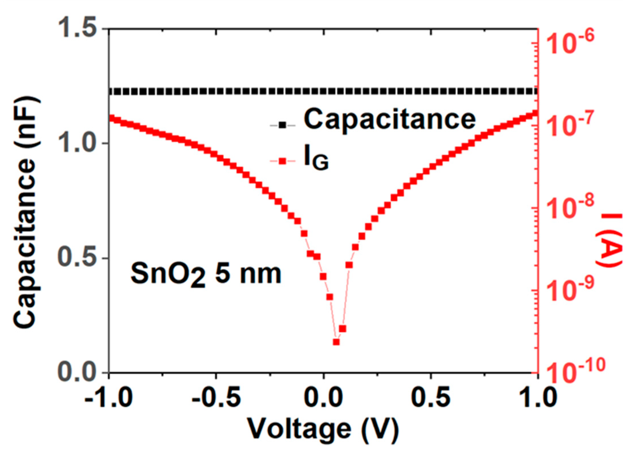

Table 1.
Comparisons of 2D semiconductor performances with our present work at Qe of 5 × 1012 cm-2.
| Semiconductor Material |
EG (eV) | meff (mo) | Dielectric Const. κ | µeff (cm2/V-s) @5 nm |
|---|---|---|---|---|
| SnON (This work) |
~3.3 | ~0.29 | 123 | 325 |
| Si [5] | 1.12 | 1.08 | 11.7 | 120 |
| MoS2 [5] | 1.8 | ~0.5 | 4~8 (2~5 layers) | 184 |
| WS2 [5] | 1.4 | 0.33 | - | 234 |
| InGaAs [5] | 0.75 | 0.042 | 12.9 | 200 |
Disclaimer/Publisher’s Note: The statements, opinions and data contained in all publications are solely those of the individual author(s) and contributor(s) and not of MDPI and/or the editor(s). MDPI and/or the editor(s) disclaim responsibility for any injury to people or property resulting from any ideas, methods, instructions or products referred to in the content. |
© 2023 by the authors. Licensee MDPI, Basel, Switzerland. This article is an open access article distributed under the terms and conditions of the Creative Commons Attribution (CC BY) license (http://creativecommons.org/licenses/by/4.0/).
Copyright: This open access article is published under a Creative Commons CC BY 4.0 license, which permit the free download, distribution, and reuse, provided that the author and preprint are cited in any reuse.


