1. Introduction
The three-dimensional lidar system can be used to obtain the range and three-dimensional image of the target so that it is widely used in space target detection, landscape mapping, underwater target detection, unmanned car driving and other fields[
1]. Among various lidar systems, the range-gated lidar system is one of the lidar systems that can penetrate scattering media such as fog, smoke, snow and water to obtain two-dimensional photos of the target and then achieve the three-dimensional reconstruction of the target[
2,
3]. In 2004, the Danish Defense Research Establishment designed the first narrow-gate high-precision, high-speed 3D imaging lidar system, which acquires the sequence slice images of the target through multiple imaging, and then weights the sequence image to recover the 3D image of the target[
4]. In 2006, J. F. Andersen introduced Raman scattering fiber and spectrometer on the basis of the original system to realize a multispectral three-dimensional imaging system with submillimeter resolution[
5]. At this point, general range-gated lidar systems have been completed, and the research on the range-gated lidar system has begun to turn to image processing. Common range-gated lidars using high-gain ICCD cameras with their switch are generally used for slice imaging due to the demand to achieve narrow switches for gated imaging. However, because of the shortcomings of multiple electro-optical conversions, low quantum efficiency and low lateral resolution caused by pixel coupling in the imaging process of ICCD cameras [
6,
7,
8], various distance-gated lidar systems that use electro-optical crystals as optical switches or modulators, and cameras with high-resolution, high-quantum efficiency and low-cost imaging devices such as MCCD (micro-polarizer camera), EMCCD (electron multiplication CCD), SCMOS. In 2016, Sungeun Jo et al. in South Korea proposed a high-precision 3D imaging lidar system consisting of a polarization-modulating Pockels cell (PMPC) and an MCCD, which can achieve a ranging accuracy of 5.2mm at 16m[
9]. In 2017, Chen Zhen et al. of the Chinese Academy of Sciences proposed a flash lidar system based on polarization modulation using two EMCCD cameras and two PMPCs, which can achieve a ranging accuracy of 0.26m in a field of view of 0.92mrad at 200m[
10]. In 2019, Wang Shengjie et al. of the Chinese Academy of Sciences proposed a high-precision correction algorithm for large field-of-view based on the lidar system proposed by Chen Zhen et al., which reduced the distance error of the system to less than 0.1m within 0.92mrad field of view[
11]. In 2020, Song Yishuo et al. from the Space Engineering University proposed a lidar system using two KTN crystals and two CCD cameras, which is characterized by a large field of view imaging and range accuracy of 4.4cm for targets 15m away under a field of view of 0.35rad[
12]. In the distance-gated lidar system designed in this paper, we choose to use a SCMOS camera as an imaging device. Compared with the ICCD commonly used in general range-gated lidar systems, the advantages of SCMOS is that it has a better signal-to-noise ratio in non-very-low light conditions, better lateral resolution, longer service life and more excellent resistance to mechanical shock[
13]. Compared with EMCCD cameras, SCMOS cameras have a higher signal-to-noise ratio, faster readout speed and higher real-time imaging frame rate at the same exposure time. Moreover, SCMOS cameras have the lowest price among the three cameras.
However, simply using a SCMOS camera is unable to achieve high-precision range-gated slice imaging as the SCMOS camera itself does not have a high-speed optical switch. It is necessary to add a high-speed switch to the SCMOS camera to enable the system to achieve range-gated slice imaging.
This paper uses the LiNbO3 (LN) crystal and two polarizers placed vertically before and after the crystal as an electro-optical switch. The standard deviation of the range calculated using the original slice images method is 3.86cm. In comparison, the standard deviation calculated using the slice images compensated by the compensation method is 2.86cm at a field of view of 2.6mrad, which verified the validity of the compensation method.
2. Distance-Gating Lidar Utilizing an Electro-Optical Crystal as the Optical Switch
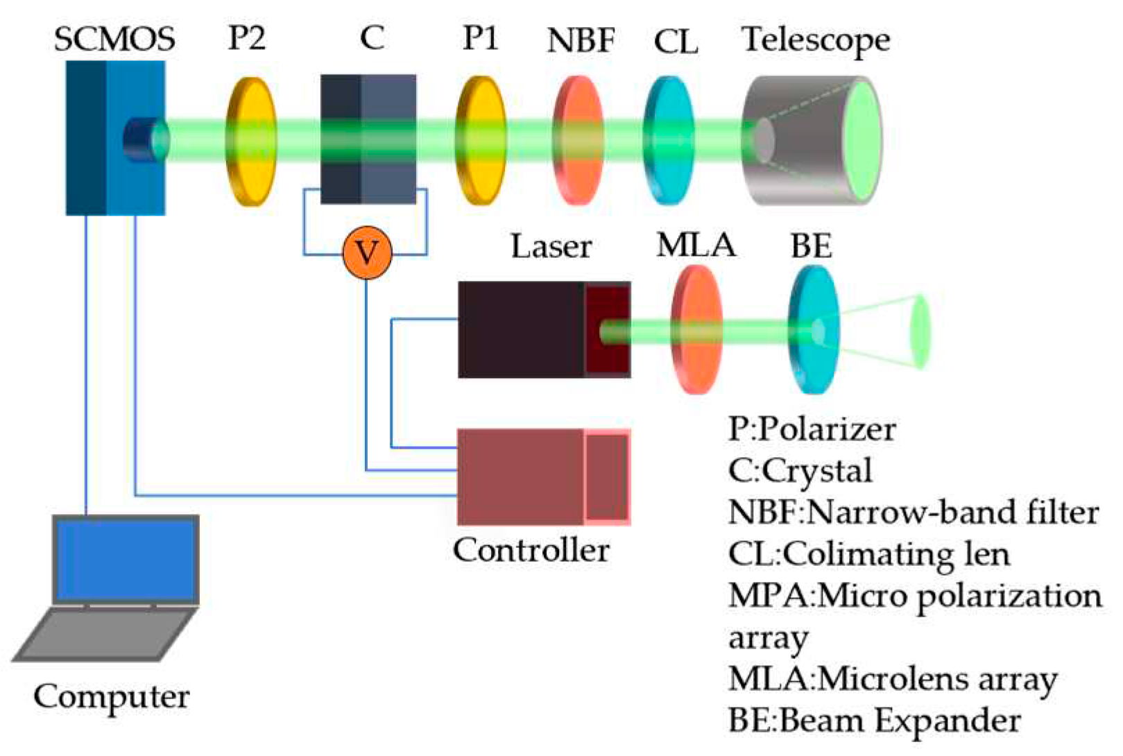
The schematic diagram of the structure of the range-gated lidar system using an electro-optical crystal as an optical switch is shown in
Figure 1. The system consists of a SCMOS camera, 2 polarizers, an electro-optical crystal, a narrow-band filter, a collimator, a receiving optical system, a pulsed laser, a microlens array, a beam expander, a delay signal generator and a computer. Among them, the polarizer (P1 in
Figure 1), the analyzer (P2 in
Figure 1), whose polarization direction is perpendicular to the polarizer, and the electro-optical crystal constitute a crystal optical switch. The optical path can be switched on and off by changing the applied voltage of the crystal. The laser is a low-repetition-rate, high-pulse-energy and narrow-pulse-width pulsed solid-state laser with a wavelength of 532nm.
When the lidar system is works, a homogeneous and expanded pulse laser beam is emitted to the target. When the pulse laser travels between the target and the receiving system, the applied voltage of the LN crystal is zero. Currently, the optical switch closed state to prevent atmospheric backscattering and non-target scattering light. After the delay time , when the reflected light of the target returns to the receiving system, the stray light of other bands is filtered out firstly by the NBF (narrow-band filter), and then under the control of the delay signal generator, a pulse voltage with pulse width is and a pulse peak of half-wave voltage of the LN crystal is added at both ends of the crystal.
At this time, the crystal electro-optical switch is on, and the SCMOS camera receives the reflected light of the target. After this process, the system completes the imaging of the target. The corresponding slice depth of field is:
where c is the speed of light, and we can see that the crystal optical switch is only turned on for a short time from the formula so that the picture obtained by the SCMOS camera corresponds to a certain distance information. A series of distance slice images can be obtained by changing the delay time
. The distance information of each image pixel can be calculated through the temporal and energy relationships between different slices. Then the three-dimensional image of the interest target can be obtained[
14].
The mainstream ranging algorithm is the weighted average method[
15]. This method is to multiply each gray value of the slice image sequence of the same pixel by a delay time serial number weight and divide it by the sum of all serial numbers to obtain an average image serial number. The average serial number is multiplied by the delay step and the delay time corresponding to the first image as the flight time corresponding to the target distance to calculate the distance, which has the advantages of high precision and fast operation speed.
According to the ranging principle above, the distance corresponding to the
ith image in the slice sequence image is:
where
represents the delay time corresponding to the
ith image,
represents the initial delay time, and
is the delay step. The average image serial numbers can be obtained:
where
represents the gray value of each pixel in the
ith image. The range corresponding to each pixel can be obtained through the following formula:
When the range of the target point is determined, according to the geometric relationship between the target image, imaging optical system and the target, the spatial position of the target point can be obtained, and the coordinates of each target point obtained can be converted in three-dimensional coordinates, and then the three-dimensional image of the target can be obtained by display processing.
3. Analysis of Electro-Optic Crystal Switch Inhomogeneity
We used a SCMOS camera to acquire the target image in our lidar system. As mentioned above, the SCMOS camera itself does not have a high-speed switch and thus can only obtain grayscale information, so it is necessary to use an optical switch composed of electro-optical crystal and two polarizers to achieve slice imaging so that the gray value of the image can correspond to a certain distance information.
The electro-optic crystal can be used as an optical switch mainly due to its conoscopic interference effect. The normalized light intensity of the central conoscopic interference pattern generated by the light passing through the optical switch is 0 theoretically when the voltage applied to the electro-optic crystal is 0. The electro-optic crystal optical switch can be regarded as an “off” state. Theoretically, the normalized light intensity of the central conoscopic interference pattern generated by the light passing through the optical switch is 1 when the voltage applied to the electro-optic crystal is half-wave. The electro-optic crystal optical switch can be regarded as an “on” state at this time. Compared with the switch of the ICCD cameras, the distribution of the conoscopic interference ring generated by the electro-optic crystal is not uniform, resulting in a deviation between the gray value of the image generated by the SCMOS cameras with electro-optic crystal switches and the SCMOS cameras with ideal switches. As can be seen from Equation (7) above, an electro-optic crystal switch will cause errors in the image sequence’s calculated mean, affecting the lidar system’s performance. An appropriate field of view needs to be selected to reduce this effect.
We choose LN crystal as the electro-optic switch, and the inhomogeneity of LN crystal was analyzed below. Combined with the light tracing analysis of the crystal with reference[
16], we can conclude that when the light travels along the crystal optical axis, the crystal phase difference delay caused by the electro-optic effect is:
The crystal conoscopic interference light intensity expression is:
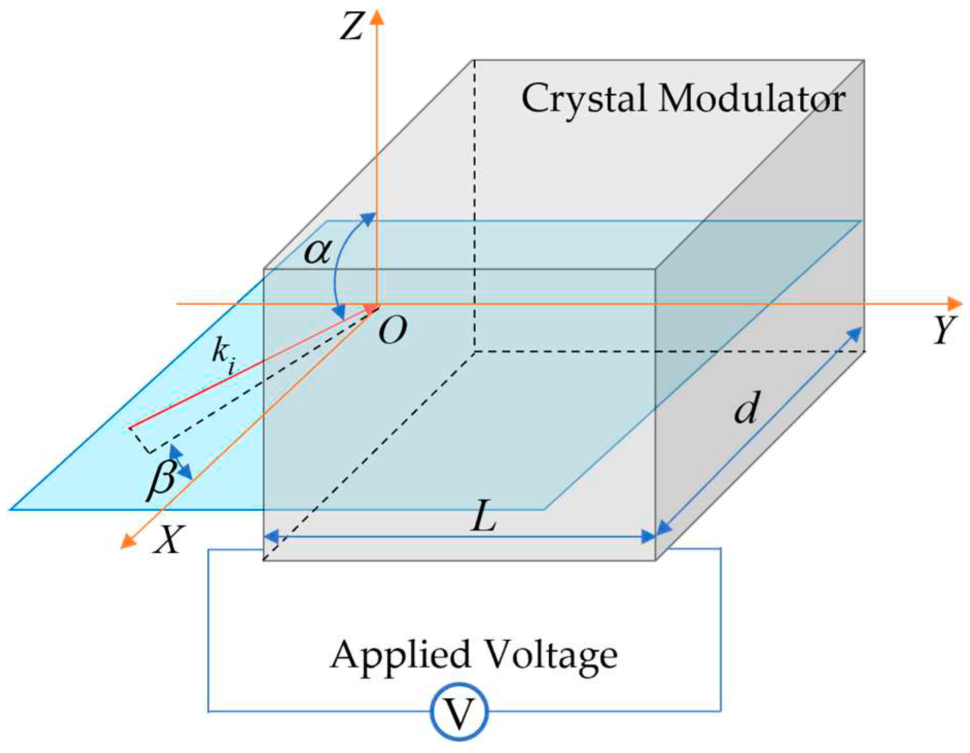
Where is the zenith angle of the light incident to the electro-optical crystal, is the azimuth angle of the incident light, V is the applied voltage of the crystal, is the refractive index of ordinary light in the crystal, is the electro-optical coefficient of the crystal, L and d are the length and thickness in the direction of applied pulse voltage, respectively. It can be seen that the ordinary light refractive index , electro-optical coefficient , length L and thickness d of the crystal are fixed values for a certain crystal, so the light intensity of the crystal is a function of , , V as variables. The influencing factors of the light intensity inhomogeneity of crystal switches are also mainly derived from , , V.
Figure 4.
Schematic diagram of the angle of light incident on the crystal surface.
Figure 4.
Schematic diagram of the angle of light incident on the crystal surface.
The influence of light intensity inhomogeneity is divided according to the abovementioned variables. The total inhomogeneity coefficient
is defined here, which represents the difference between the actual normalized light intensity received by a pixel on the detector and the normalized light intensity of the corresponding pixel in the center of the field of view on the detector, that is, the difference between the transmittance of the crystal optical switch of the pixel in the center of the field of view and the transmittance of the crystal optical switch corresponding to any other pixel. The inhomogeneity coefficient caused by the difference of incidence angle
、
is defined as
, representing the difference in transmittance of the crystal optical switch due to the influence of the conscopic light interference effect; The inhomogeneity coefficient caused by the unideal pulse voltage
V is defined as
, the difference between the transmittance of the crystal under the actual non-ideal pulse voltage and the ideal pulse voltage. The total inhomogeneity coefficient is the sum of the two factors:
3.1. Analysis of Inhomogeneity Caused by the Angle of Incident Light of the Crystal
Firstly, the inhomogeneity caused by the different angles
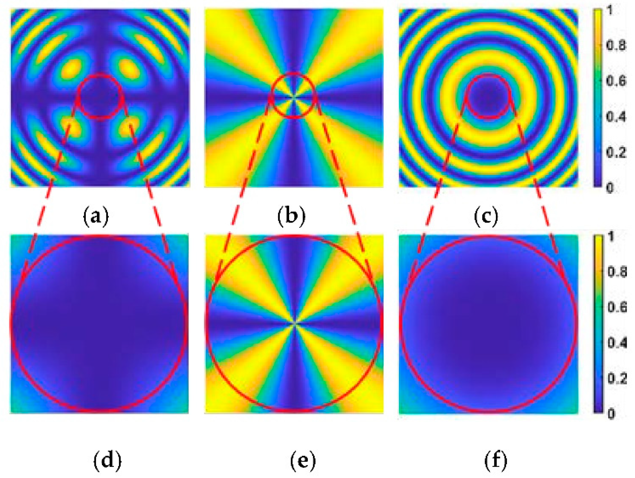
of the crystal incident light is analyzed. According to Equation (10), the interference pattern of the crystal under ideal conditions is calculated and simulated, and the simulation result is shown in the following
Figure 5:
As shown in
Figure 5,
Figure 5a is the distribution of normalized light intensity within a 69.8mard field of view after the light passes through the crystal when the voltage
V applied across the crystal is 0.
Figure 5b,c show the influence of polarization direction on light intensity and the influence of
phase difference
on the light intensity, respectively. The 17.5mrad field of view region in figures (a), (b) and (c) is enlarged to obtain figures (d), (e) and (f). It can be seen from
Figure 5d that the homogeneity of the image center is good, while the image uniformity in the field edge area of the field of view in the azimuth angle of 45°, 135°, 225° and 315° is poor.
Through the simulation data analysis, the light intensity per pixel in
Figure 5d within the field of view of 17.5mrad is less than 0.07, and the crystal switch is considered to be in the “off” state at this time.
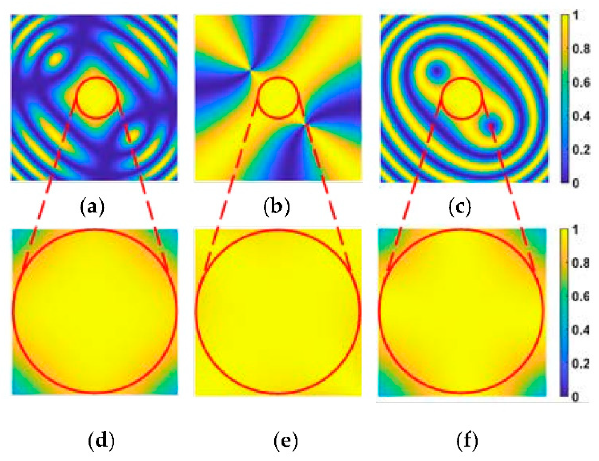
The voltage across the crystal is set to a half-wave voltage during the simulation of
Figure 4, and the simulation results are shown in
Figure 5:
Figure 6d The light at each pixel within the 17.5mrad field of view is greater than 0.87, which the crystal switch is considered to be in the “on” state at this time, but the aberration in the edge area of the field of view is nonnegligible.
According to the interference intensity formula, the source of inhomogeneity error is analyzed. The range of light intensity is 0.95 ~ 1 in
Figure 6e and the range of light intensity is 0.86 ~ 1
Figure 6f. Therefore, the polarization direction
has less effect on the light intensity in the 17.5mrad field of view compared to phase difference
.
When the voltage applied to the crystal is 0, the electro-optical crystal switch is in the “off” state, and the phase difference between the center part and the edge within the 17.5mrad field of view is small so that the impact on imaging is negligible. When the electro-optical crystal switch is in the “on” state, the error caused by the polarization direction
is small, so the interference light intensity can be approximated as an expression of phase difference:
When the voltage applied to the crystal is a half-wave voltage, the electro-optical crystal switch is in the “on” state, and the ideal interference light intensity value should be 1 within the entire field of view of the electro-optical crystal switch. At this time the phase difference of each point of imaging on the detector should be
, and at each point outside the center point of the field of view, the corresponding light intensity inhomogeneity coefficient is:
3.2. Analysis of Inhomogeneity Caused by Unideal Pulse Voltage Applied to the Crystal
The inhomogeneity caused by the pulse voltage V applied to the crystal is analyzed below.
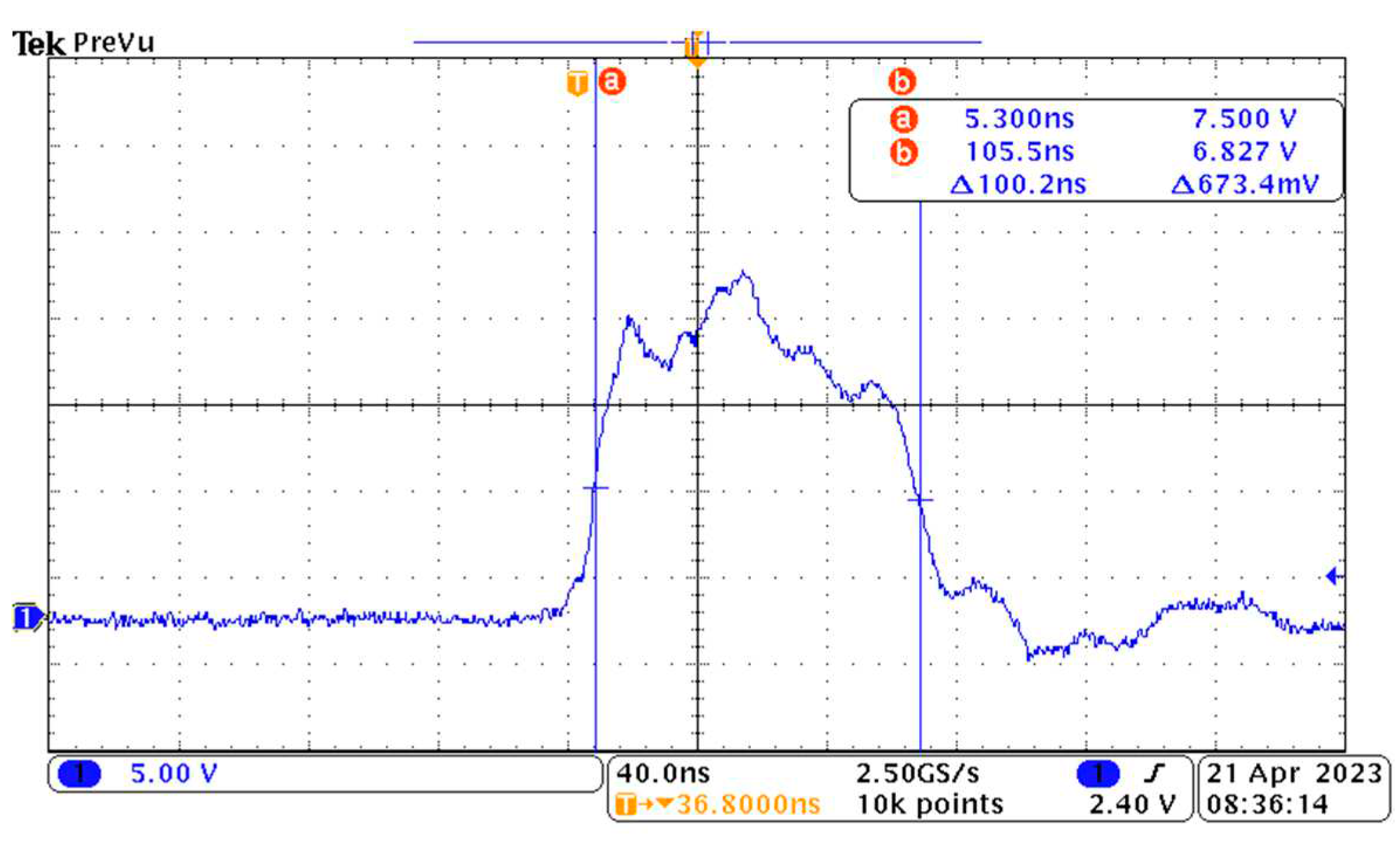
In order to calculate the inhomogeneity caused by pulse voltage, the pulse voltage applied to the electro-optical crystal should be measured with an oscilloscope. It can be seen from the measurement results below that the pulse width of the applied voltage source used in this research group is 100 ns.
Figure 7.
Image of the applied voltage of the crystal detected by the oscilloscope.
Figure 7.
Image of the applied voltage of the crystal detected by the oscilloscope.
Combined with Equation (10), the conscopic interference pattern produced by the crystal is a function of voltage, and the corresponding conscopic interference pattern is different for different voltages. The light intensity distribution detected on the detector during the process of applying a half-wave pulse voltage to the electro-optical crystal without considering the laser pulse waveform is:
Among them, represents the light intensity of the image detected by the detector after one exposure, represents the voltage value of the ith sampling point on the oscilloscope, n is the total number of the laser pulse voltage sampling points on the oscilloscope, represents the light intensity corresponding to the crystal conscopic interference pattern when the voltage applied to the crystal is , and represents the normalized light intensity of the laser pulse received by the crystal when the voltage is .
The inhomogeneity coefficient corresponding to the error caused by the non-ideal pulse voltage is
In this formula, is the half-wave voltage of the crystal and is the normalized conoscopic interference light intensity corresponding to the half-wave voltage.
Combining the influence of the conoscopic interference effect of LN crystal and the non ideal pulse voltage, the total inhomogeneity coefficient generated by the electro-optic crystal optical switch can be obtained by bringing Formula (9) and Formula (11) into Formula (7):
3.3. A compensation Method for Crystal Inhomogeneity
According to the above analysis of the source of electro-optical crystal switch inhomogeneity, the compensation method of crystal inhomogeneity is studied. In the actual compensation process, not only the relationship between the crystal ideal matrix, the inhomogeneity matrix and the compensation matrix should be considered, but also a certain extinction ratio of the switch should be taken into consideration as the actual switch is not ideal.
We define the transmittance matrix represented by
as the full
matrix, and
represents the transmittance of the ideal switch under a certain voltage applied to the crystal. The actual electro-optic crystal switch transmittance matrix is defined as
,and the transmittance of the center field of view in
should also be
, the inhomogeneity matrix calculated by the above formula (12) is defined as
, the actual inhomogeneity matrix considering the extinction ratio is defined as
,the compensation matrix is
C ,and the extinction ratio matrix is defined as
. Then
can be calculated by the following formula
In the formula above,
represents a matrix with all values of 1,
is the maximum value function, which is used to normalize the matrix. After obtaining the actual inhomogeneity matrix, the compensation matrix
can be calculated through the following formula :
For the slice image captured by the experimental lidar system, the image compensating the inhomogeneity of the electro-optic crystal switch can be obtained by multiplying the pixel by pixel with the corresponding compensation matrix. It should be noted here that according to formula (1), the slice image obtained has a certain depth of field, meaning that a slice image may contain laser pulses reflected by targets at different distances. The time of flight of the laser pulse reflected from different distances is different, and the applied pulse voltage of the crystal corresponding to the laser pulse received by the system at different times is also different, resulting in different transmittance of the electro-optic crystal switch. When the pulse width of pulse voltage applied to the crystal and the laser pulse width of the crystal are large, the interference state of the electro-optic crystal switch corresponding to the target at different distances on a single slice image is quite different. At this time, when the compensation matrix corresponding to a specific time is applied to the slice image, a more significant error might be introduced. The compensation matrix can only be used when the laser pulse width and the pulse width of the voltage applied to the crystal are small to a certain extent.
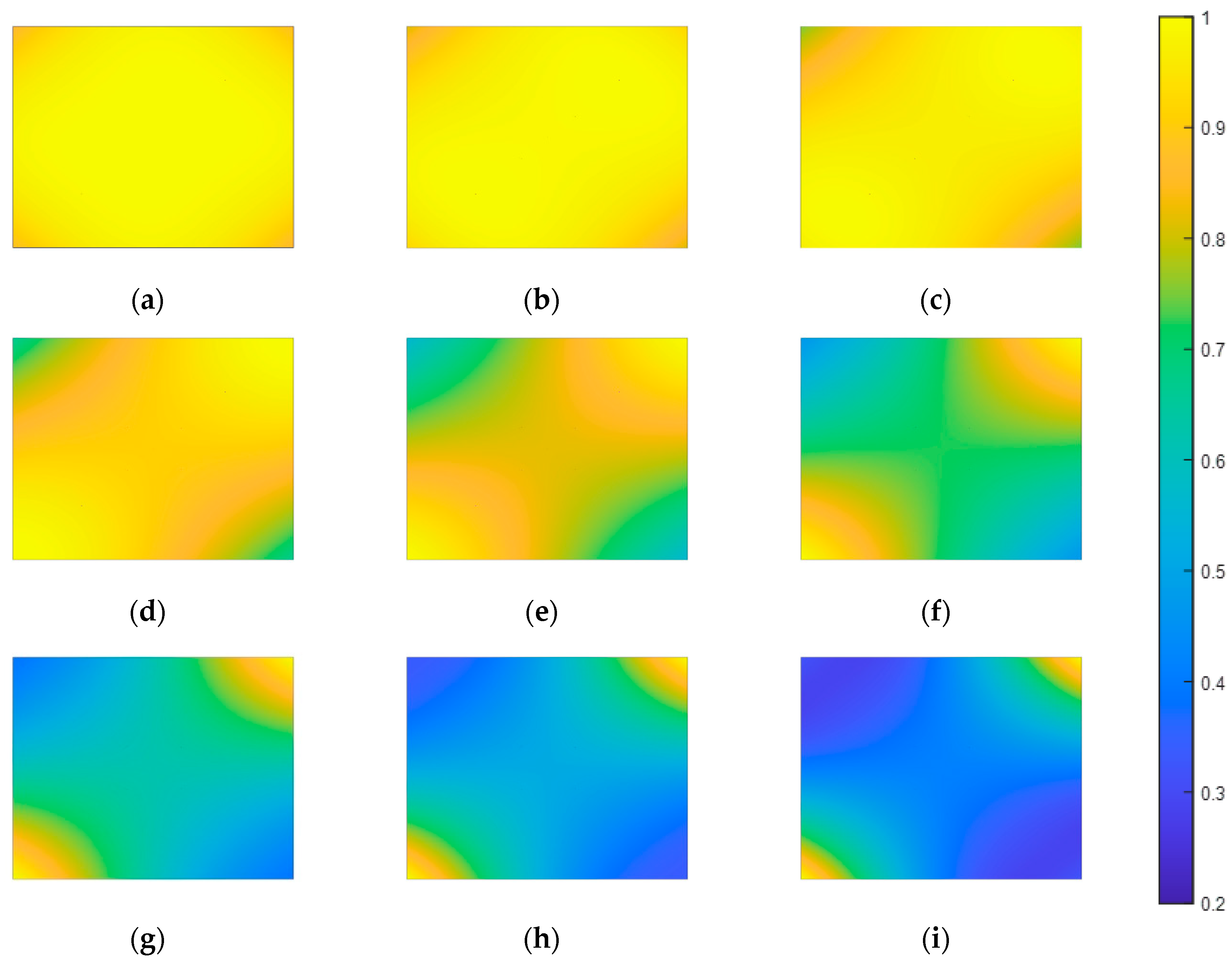
Figure 9 shows the results of gated imaging of planar targets by a range gated lidar system using LN crystal as a switch under ideal conditions. The relationship between the pulse voltage applied to the crystal and the laser pulse corresponding to the simulated imaging results in
Figure 9a is shown in
Figure 8a. And (b), (c), (d), (e), (f), (g), (h) and (i) are the simulation images corresponding to the increase of the gating delay by 4ns, respectively. The relationship between the pulse voltage applied to the crystal and the laser pulse corresponding to the simulated imaging results in
Figure 9i is shown in
Figure 8b. Combined with
Figure 8, when the laser pulse entirely coincides with the pulse voltage applied to the crystal in time sequence, within a 2.6mrad field of view, the maximum normalized light intensity in the simulation
Figure 9a is 1, and the minimum normalized light intensity is 0.96, which can be regarded as the case where the plane target is completely gated. With the increase of the delay time, the coincidence region of the laser pulse and the pulse voltage applied to the crystal gradually decreases, and only part of the laser pulse is gated. The normalized light intensity of the image imaging decreases from both ends to the center, and the normalized light intensity of the image’s upper left and the lower right end is significantly higher than that of the lower left and upper right end. The simulation results reflect the apparent inhomogeneity of the system slice image.
Figure 8.
The temporal relationship between the laser pulse and the voltage applied to the crystal. The purple region represents the laser pulse voltage, the orange region represents the laser pulse, and the gray region represents the coincidence region of the laser pulse and voltage applied to the crystal. Figure (a) indicates that the laser pulse and the applied pulse voltage are completely coincident. Figure (b) indicates that the laser pulse partially leaves the applied pulse voltage of the crystal.
Figure 9.
2.6mrad field of view angle of the system simulation results of the plane target imaging.
Figure 9.
2.6mrad field of view angle of the system simulation results of the plane target imaging.
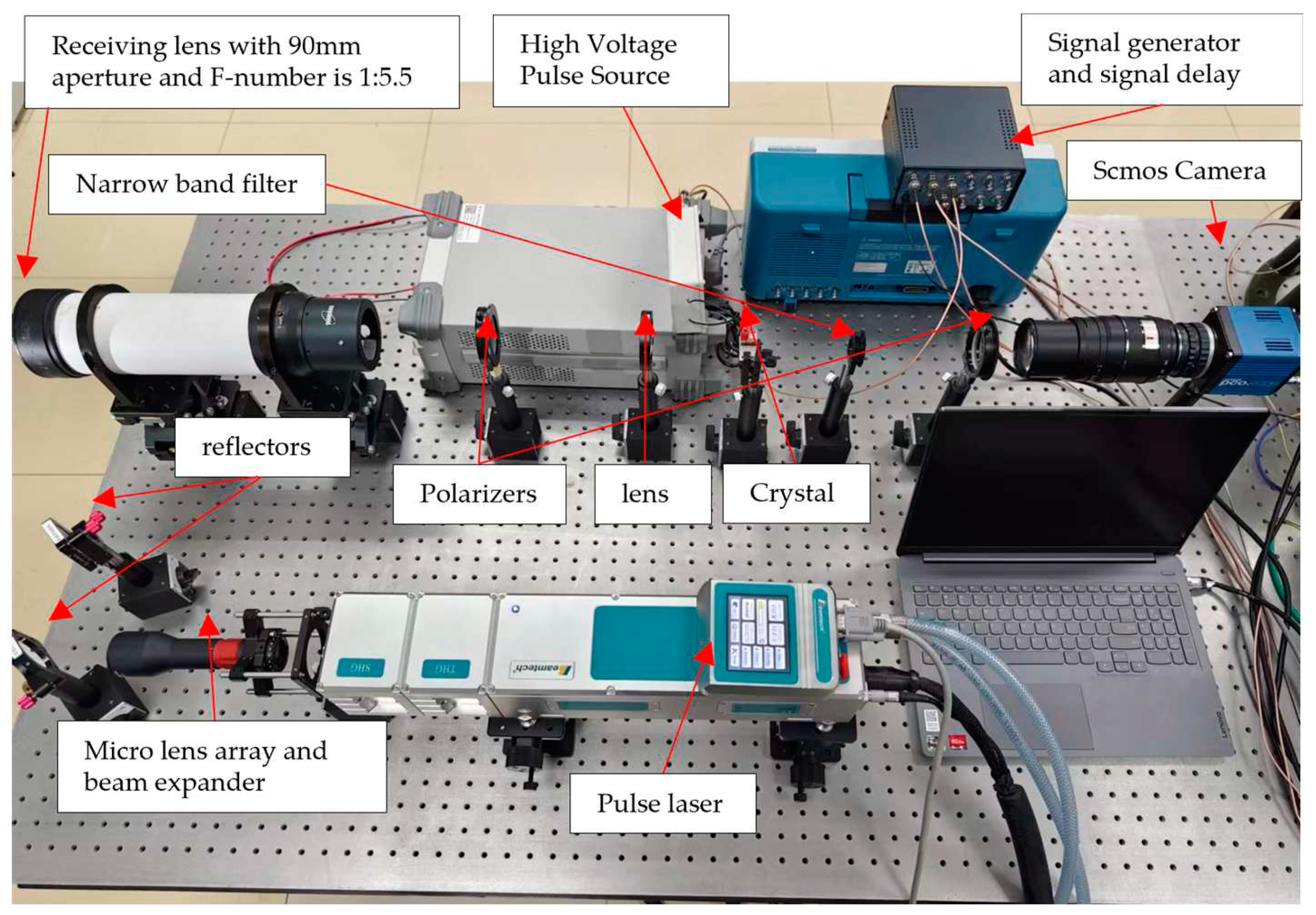
Figure 9.
The range-gated experimental lidar system using an LN crystal as optical switch.
Figure 9.
The range-gated experimental lidar system using an LN crystal as optical switch.
4. Experiment and Analysis
We use a signal generator and a signal delayer to realize the synchronous control of the crystal voltage source, SCMOS camera exposure control, laser pulse xenon lamp signal and Q-switched signal.
Table 1.
Main parameters of range-gated experimental lidar system using an LN crystal as an optical switch.
Table 1.
Main parameters of range-gated experimental lidar system using an LN crystal as an optical switch.
| Parameter |
Value |
| Wavelength |
532 nm |
| Pulse Energy |
200 mJ |
| Pulse Width |
7 ns |
| Pulse Repetition Frequency |
5 Hz |
| Aperture |
400 mm |
| Detector |
2160 2560 pixels |
Since Tektronix ‘s AFG 31000 SERIES arbitrary signal generator(ASG) we use outputs up to two signals and the Fastlaser.Tech ‘s TDG-VII timing delay generator(TDG) we use produces a delay of up to 1ms, which is less than the exposure delay of the PCO Edge.55 SCMOS camera, and TDG-VII’s jitter time in the external trigger mode is much smaller than the corresponding jitter time when using the internal clock, so we choose to combine the signal generator and the signal delayer to achieve synchronization control of the entire experimental system. We use a pulsed xenon lamp pumped Nd: YAG Q-switched laser as the illumination source. When the system works, the signal generator first generates a non-delay signal to trigger the exposure control of the SCMOS camera at a frequency of 5 Hz. Then the ASG generates a signal triggering TDG after the SCMOS camera exposure trigger delay time . The signal delayer generates three signals at this time. The first two signals are non-delay signals with a frequency of 5 Hz, which trigger the laser ‘s xenon lamp signal and Q-switched signal, respectively. The latter signal is a signal with a delay of and a frequency of 5Hz, which is used to trigger the external high-voltage source of the LN crystal. When the laser is triggered, the laser emits a pulsed laser with a frequency of 5Hz and a pulse width of 7ns to the target. After the emitted laser is homogenized by the microlens array and expanded by the beam expander, it is directed to the target through two mirrors used to adjust the laser emission direction. The scattered light of the target is received by a lens with an aperture of 90 mm and an F-number of 1:5.5 and collimated by a lens with a focal length of 75 mm. Behind the lens is an LN crystal with a length and width of 9mm and a thickness of 18mm. When the external pulse high-voltage source of the LN crystal is triggered by the third signal generated by the TDG, a high-voltage pulse power supply is added at both ends of the crystal to make the crystal optical switch turn on, so as to realize the gating imaging of the interest target.
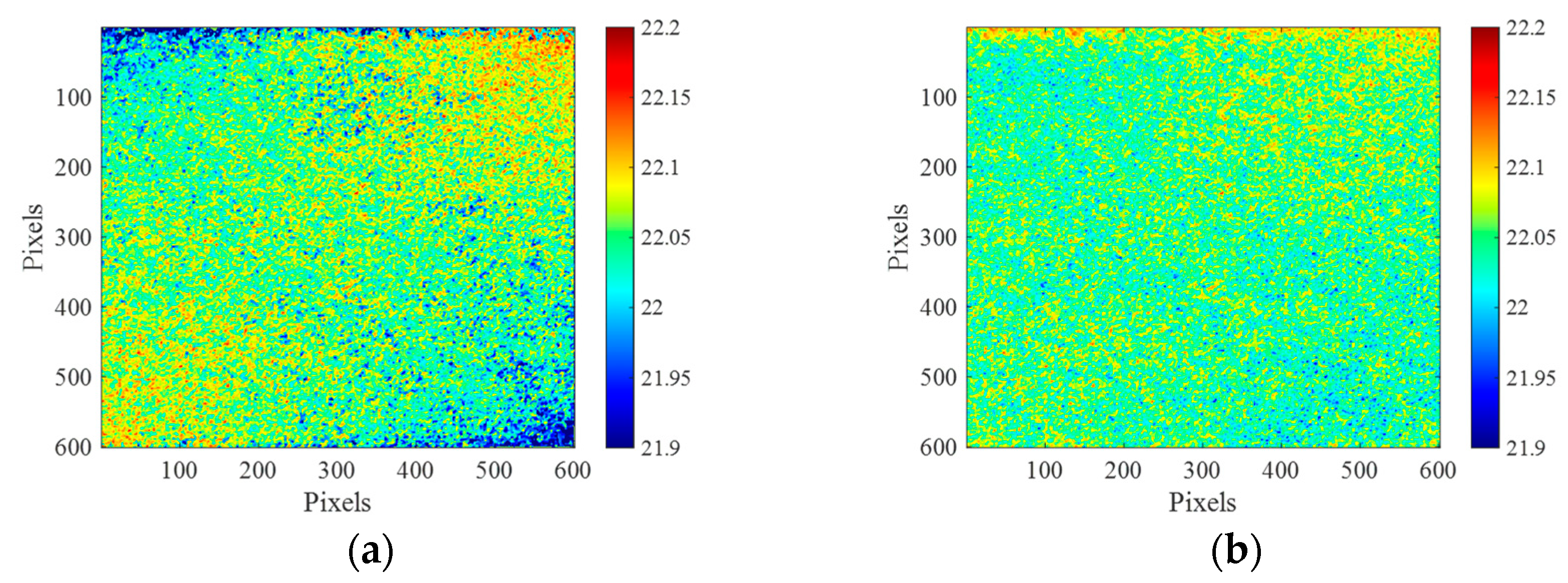
In order to verify the accuracy of the compensation method, a pure white plate is placed 22.04 meters away from the receiving system, and a gating imaging experiment to the white plate is conducted. The effect of imaging compensation is shown in
Figure 10. From
Figure 10a, we can see that because the physical principle of the crystal as an optical switch is the conoscopic interference effect of the crystal, only the area of about 301
301 pixels in the center of the field of view can achieve uniform imaging.
Figure 10c,d are the contrast images of the imaging effect of the 601
601 pixels range area of the crystal center before and after compensation. From the image effect before and after compensation, it can be seen that in the pixel area taken, the gray image uniformity of the target imaging is significantly improved, proving the algorithm’s accuracy.
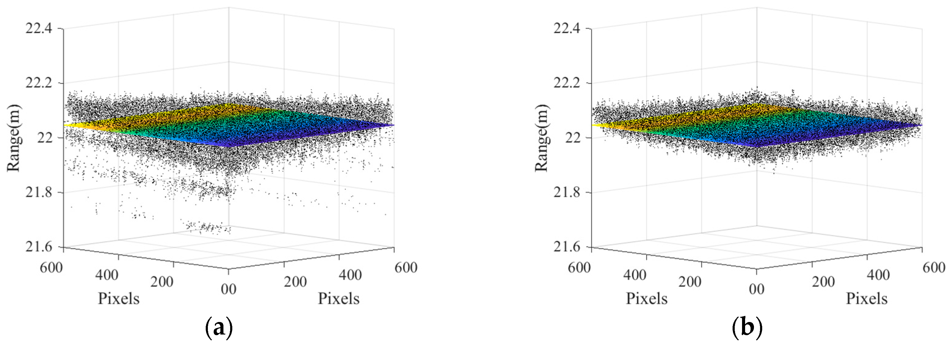
Using the slice image before compensation and the slice image after compensation for three-dimensional reconstruction, the obtained point cloud image is as follows :
Figure 13 shows the comparison of the distance depth with the horizontal row of pixels, where the orange curve represents the distance depth curve in
Figure 12a, the green curve represents the distance depth curve in
Figure 12b, and the blue line represents the true distance of the target.
Figure 13a–c represent the average distance depth of the first to fifth rows of pixels in
Figure 12, the average distance depth of the 299th to 303rd row of pixels, and the average distance depth of the 597th to 601st rows of pixels. From
Figure 11,
Figure 12 and
Figure 13, we can conclude that due to the influence of the inhomogeneity of the electro-optical crystal switch, the calculated value of the distance depth is generally smaller than the true value in the upper left and lower right parts of the distance depth image calculated by the original slice image, while the calculated value of the distance depth is generally larger than the true value in the lower left and upper right sides of the image. And there are obvious isolated points in the edge of the point cloud image. The range accuracy of the depth image restored by the compensated slice image is significantly improved in the corner part, the tilt phenomenon is obviously suppressed, the isolated points of the image in the edge part are significantly reduced, and the image dispersion in the center part is reduced. This result verifies the accuracy of the compensation method.
The distance accuracy of the image within a 2.6 mrad field of view is calculated using the formula as follows:
In the formula,
represents the standard deviation of distance depth.,
n represents the total number of pixels,
represents the distance corresponding to the ith pixel,
represents the actual measured target distance, and takes the fixed value of 22.04 meters. After calculation, the standard deviations of the distance depth corresponding to
Figure 12a and
Figure 12b are 3.86 cm and 2.86 cm, respectively. The leading causes of ranging error are as follows. First, the pulse voltage applied to the crystal is not an ideal pulse, and its peak waveform stability is poor. In this case, there will be errors when the sequence image weighted average method is used to recover the distance depth. Second, the principle of the crystal as an optical switch is the conoscopic interference effect of the crystal. The conoscopic light interference effect itself has inhomogeneity, and there will be a significant error at the edge of the field of view. Third, the jitter time of the TDG triggering the crystal pulse voltage is 25ps according to the product manual, and the corresponding ranging error is 0.38 cm. The shot noise of SCMOS will also cause a particular distance error. After compensation, the influence of the first and the second reason is obviously suppressed, and the standard deviation of system distance depth is obviously improved.
5. Conclusions
In this paper, a range-gated lidar system using an electro-optic crystal as the optical switch is designed. The slice image of the target is obtained by synchronously controlling the pulse voltage applied to the crystal, laser pulse and SCMOS exposure, and then the three-dimensional point cloud image and distance depth image of the target are reconstructed using the slice image.
Compared with the traditional range-gated lidar system using ICCD as an imaging device, a high-precision timing control circuit and high-bandwidth detector must be used to improve the range accuracy. For the system designed in this paper, the use of the SCMOS detector only needs to detect the intensity of the reflected laser of the target, instead of detecting the time of flight (TOF), and does not require a high-precision timing control circuit, which greatly saves the cost of the system.
However, compared with the shutter built-in ICCD, the use of an electro-optic crystal as light shutter will introduce new inhomogeneity errors, which will affect the ranging accuracy of the system. To reduce the impact of this error, this paper quantitatively analyzes the source of the crystal inhomogeneity error, proposes a compensation method for crystal inhomogeneity, and gives the mathematical expression of the inhomogeneity compensation matrix. The experimental results show that compared with the range depth image restored by the original slice image, the accuracy of the compensated range depth image is significantly improved, and the standard deviation of the range depth is reduced from 3.86 cm to 2.86 cm within 2.6 mrad field of view, which verifies the accuracy of the algorithm and provides a guarantee for further improving the performance of the system.
References
- Park, J.; Cho, J.; Lee, S.; et al. An Automotive LiDAR Performance Test Method in Dynamic Driving Conditions. Sensors 2023, 23, 3892. [Google Scholar] [CrossRef] [PubMed]
- Sun, L.; Sun, D.; Sun, C.; et al. 3D Range-gated Imaging Method Based on Parabolic Envelope Inversion. Acta Armamentarii 2022, 43, 1868–1873. [Google Scholar]
- He, Z.; Huang, Y.; Zhang, Y.; et al. Range-Gated Imaging LiDAR by Scanning Reception of Space Light Modulator. Acta Opt. Sin. 2020, 40, 7–13. [Google Scholar]
- Busck, J.; Heiselberg, H. Gated viewing and high-accuracy three-dimensional laser radar. Appl Opt 2004, 43, 4705–4710. [Google Scholar] [CrossRef]
- Andersen, J.F.; Busck, J.; Heiselberg, H. Pulsed Raman fiber laser and multispectral imaging in three dimensions. Appl. Opt. 2006, 45, 6198–6204. [Google Scholar] [CrossRef] [PubMed]
- Denvir, D.J.; Conroy, E. Electron-multiplying CCD: The new ICCD. Low-Light-Level and Real-Time Imaging Systems, Components, and Applications 2003.
- Wenwen, Z.; Qian, C. Signal-to-noise ratio performance comparison of Electron Multiplying CCD and Intensified CCD detectors. In Proceedings of the 2009 International Conference on Image Analysis and Signal Processing, LinHai, China, 11–12 April 2009. [Google Scholar]
- Djazovski, O.; Daigle, O.; Laurin, D.; et al. Electron-multiplying CCDs for future space instruments; Photonics North, United States, 11 October.
- Jo, S.; Hong, J.K.; Bang, H.; et al. High resolution three-dimensional flash LIDAR system using a polarization modulating Pockels cell and a micro-polarizer CCD camera. Opt Express 2016, 24, A1580. [Google Scholar] [CrossRef] [PubMed]
- Chen, Z. Research on three-dimensional active imaging with polarization-modulated method. Doctor’s Thesis, University of Chinese Academy of Sciences, Xi`an China, 2017.
- Wang, S.; Liu, B.; Chen, Z.; et al. High-Precision Calibration Algorithm for Large Field-of-View Polarization-Modulated 3D Imaging. IEEE Photonics Technol. Lett. 2019, 31, 1064–1067. [Google Scholar] [CrossRef]
- Song, Y.; Zhao, J.; Wang, B.; et al. The potassium tantalate niobate (KTN) crystal-based polarization-modulated 3D ladar with a large field of view. Opt Lett 2020, 45, 5319–5322. [Google Scholar] [CrossRef]
- Capmany, J.; Torregrosa, A.J.; Maestre, H. Intracavity image upconversion system with fast and flexible electro-optic image gating based on polarization-frustrated phase-matching for range-gated applications. Opt Express 2020, 28, 1936–1953. [Google Scholar] [CrossRef] [PubMed]
- Monnin, D.; Schneider, A.L.; Christnacher, F.; et al. A 3D Outdoor Scene Scanner Based on a Night-Vision Range-Gated Active Imaging System; 3D Data Processing, Visualization, and Transmission, Third International Symposium on, United States, 2006.
- Laurenzis, M.; Christnacher, F.; Monnin, D. Long-range three-dimensional active imaging with superresolution depth mapping. Opt. Lett. 2007, 32, 3146–3148. [Google Scholar] [CrossRef] [PubMed]
- Sun, H.; Li, Y.; Guo, H.; et al. Electro-optic modulation aberration correction algorithm based on phase difference compensation. Appl. Opt. 2022, 61, 8982–8987. [Google Scholar] [CrossRef] [PubMed]
|
Disclaimer/Publisher’s Note: The statements, opinions and data contained in all publications are solely those of the individual author(s) and contributor(s) and not of MDPI and/or the editor(s). MDPI and/or the editor(s) disclaim responsibility for any injury to people or property resulting from any ideas, methods, instructions or products referred to in the content. |
© 2023 by the authors. Licensee MDPI, Basel, Switzerland. This article is an open access article distributed under the terms and conditions of the Creative Commons Attribution (CC BY) license (http://creativecommons.org/licenses/by/4.0/).
