Submitted:
31 December 2022
Posted:
03 January 2023
You are already at the latest version
Abstract
Based on the analysis of the working principle, circuit design and working loss of the common charger DC/DC converter, this paper designs a ZVS half-bridge three-level DC/DC converter based on non-phase-shift control mode, and proposes a multi-stage constant current and voltage limiting charging control strategy based on modulation wave selection control. The simulation results show that the proposed method and control strategy have faster voltage regulation ability and wider stability margin, and can achieve stable current sharing control in the charging process.
Keywords:
DC/DC Charger
; circuit design
; charging strategy
; working loss
1. Introduction
In recent years, with the rapid development of electric vehicles, their ownership has increased rapidly, and the problems of difficult charging and inconvenient charging of electric vehicles have become prominent. Due to the limited space and heat dissipation capacity in the vehicle, market users have put forward higher and higher requirements for the charging efficiency and power density of the charger [1]. According to the data of the Ministry of Public Security, as of the end of September 2022, the number of new energy vehicles in the country is 11.49 million. According to the data of the China Charging Alliance, as of June 2022, a total of 3.918 million charging infrastructures have been built nationwide. Under the background of the policy and the exponential growth trend of new energy vehicles, the national electric vehicle charging industry still has considerable market demand. The development demand of chargers is increasingly tending to high-energy rate density, low heating loss and convenient charging [2,3,4].
According to the installation location, the charger can be divided into on-board charger and off-board charger [5]. On-board charger installed in electric vehicles, generally through the household socket or AC charging pile for charging, charging voltage is usually 220kV and single-phase AC. Because the volume and weight of the vehicle charger should not be too large, and for single-phase power supply, all its output power is usually small, slow charging speed, gradually eliminated by the market [6]. At present, most electric vehicle chargers are non-vehicle chargers, whose input power is 380V three AC and output is DC. Off-board charger as the core part of the DC charging pile, its volume is not limited by space, and for three-phase power supply, so the output power is higher, the charging speed is also greatly improved, widely used [7,8,9].
According to the different working frequency, the charger can be divided into power frequency charger and high frequency charger [10]. Power frequency charger operating frequency is low, resulting in filtering problems, so the volume of the filter is usually relatively large, so that the volume of the charger will increase accordingly [11]. The high-frequency charger uses a high-frequency isolation transformer to increase the operating frequency, thereby reducing the volume of the filter and reducing the volume of the charger. However, due to the high switching frequency of the high frequency charger, it will produce a large switching loss, so it is necessary to use soft switching technology to reduce its power loss and improve work efficiency [12,13].
According to the different charging methods, electric vehicle charger can be divided into AC charger and DC charger [14]. The AC charger is limited because of its slow charging speed, while the DC charger has a fast charging speed and can provide sufficient power. The adjustment range of its output voltage and current is large, also known as ' fast charging [15]. DC charger is generally divided into two stages, AC/DC converter and DC / DC converter. The charger DC/DC converter converts the high-voltage DC obtained by rectification into low-voltage DC for battery charging, and its comprehensive performance directly affects the operating efficiency of the charger [16,17,18].
The research focus of DC/DC converter technology gradually tends to be high frequency, multi-level and soft switching. In Reference [19], an online real-time optimization charging strategy for electric vehicle chargers is proposed for charging stations with renewable energy generation. This strategy can adjust the current charging power and the charging plan in the next 24 hours according to the real-time output of renewable energy and the real-time status information of electric vehicles. The charging optimization strategy can optimize the charging cost of the charging station to a certain extent and improve the load fluctuation when the charger is charging. The multi-level DC/DC converter with high voltage level is adopted in the reference [20] to improve the charging efficiency by improving the voltage level of the charger. The control strategy combining phase shift and frequency conversion can realize wide range adjustment of output voltage. In Reference [21], aiming at the problems of passive charging, high harmonics and low power factors of electric vehicle charging piles in the current market, the active power factor correction technology and double closed-loop direct voltage control strategy are used to design the three-phase half-bridge control circuit of the charger and its PI controller parameters. The simulation results show that the control strategy can improve the charging power while ensuring that the charger has a stable output voltage. In Reference [22], the DC/DC converter of on-board charger of electric vehicle has the problems of output voltage fluctuation, large conduction loss and zero voltage switch (Zero Voltage Switch) loss. The clamping diode is used in the traditional shift-to-full-bridge DC/DC converter, and the voltage oscillation of the output rectifier tube is suppressed by the soft-switching synchronous rectification technology. The experimental results show that this method reduces the conduction loss and voltage oscillation of the rectifier tube and improves the dynamic performance of the vehicle charger.
Based on the analysis of the working principle, circuit design and working loss of the common charger DC/DC converter, this paper designs a ZVS half-bridge three-level DC/DC converter based on non-phase-shift control mode, and proposes a multi-stage constant current and voltage limiting charging control strategy based on modulation wave selection control. The simulation results show that the proposed method and control strategy have faster voltage regulation ability and wider stability margin, and can achieve stable current sharing control in the charging process.
2. Design and loss analysis of fast charging optimization circuit for DC/DC charger
2.1. Topology of ZVS half-bridge three-level DC/DC converter
The initial development of electric vehicle charger is mainly composed of linear power supply. The charging efficiency is not high, and the volume is large and the capacity is small. Until the 1970s, with the invention of IGBT tubes that can withstand high voltage and high current, the development of charger power supply reached a new level. Switching power supply has become the mainstream of high power charger because of its high efficiency and high power density. Because the market demand for fast charging of electric vehicles has been very urgent, the charging power requirements of on-board chargers are increasing day by day, and modular design has become the mainstream development trend of chargers. At present, the dominant high-power DC/DC charger in the market is usually composed of a front-end AC/DC rectifier with power factor correction function and a rear-end DC/DC converter that controls the charging power. The structure is shown in Figure 1.
The common front-stage rectifier part is mainly active (three-phase three-level PWM rectifier) topology, its function is mainly to correct the power factor. The main functions of the post-stage DC/DC converter are charging power control and voltage isolation. Therefore, the working efficiency of the post-stage DC/DC converter determines the overall performance of the DC/DC charger. The DC/DC converter controlled by the traditional pulse width modulation method belongs to the hard switching type, that is, the voltage and current at both ends of the switch tube are not zero during the conduction and shutdown, and there is a cross between the two. The switching loss is caused by this cross section. As the frequency increases, the switching loss will increase, and the switching process will produce a large peak voltage and switching noise, resulting in more serious electromagnetic interference problems. The switching process is shown in Figure 2.
Soft switch is by adding inductance and capacitance to the circuit, using resonance to change the period of voltage and current, which can eliminate the cross part of voltage and current in the process of hard switching, a good solution to the switching loss, noise interference and other issues, the switching process is shown in Figure 3.
At present, there are three main types of soft-switching DC/DC converters on the market : zero-switching PWM, zero-switching PWM and harmonic mode converter. Zero-switching PWM converter includes zero current switching (ZCS) converter and zero voltage switching (ZVS) converter. In this paper, a three-level DC/DC charger model based on ZVS half-bridge is designed and its loss is analyzed, which greatly improves the charging efficiency and power density of the charger. The topology is shown in Figure 4.
In the above Figure, Vin is the input voltage of the ZVS half-bridge three-level DC/DC converter. C1 and C2 are large-capacity input capacitors and their values are equal. Q1 and Q2 form the upper arm, and Q3 and Q4 form the lower arm. D1 ~ D4 are reverse parallel body diodes, which provide freewheeling paths for each mode. D5 and D6 are neutral point clamped diodes, whose role is to make the voltage clamp at the midpoint of the capacitor, so that the voltage of point A and point B has three states: +Vin, 0 and -Vin. Tr is ZVS half-bridge three-level DC/DC converter transformer, the role is mainly for electrical isolation and voltage conversion. The secondary full-bridge rectifier circuit of the converter is composed of DR1 ~ DR4, which outputs DC pulse voltage to C and D points. Cr1 ~ Cr4 are resonant capacitors and Lr is resonant inductor. Cf is the output filter capacitor and Lf is the output filter inductor. Their main functions are energy storage and filtering. Cf and Lf optimize the rectified DC pulse voltage to a DC voltage with small ripple, providing stable energy to the load. The relationship between input and output of the converter is:
In the above equation, D represents the duty cycle and has D = 2Ton/Ts, Ton represents the turn-on time, Vin represents the voltage between point A and point B, K represents the turn ratio of the primary and secondary sides of the transformer. The output voltage is controlled by adjusting the values of D and K, and the duty cycle of the switch tube must be limited to 0.5.
2.2. PWM control of ZVS half-bridge three-level DC/DC converter
In the working process of the converter, by controlling the simultaneous conduction of Q1 and Q2 or Q3 and Q4, the pulse voltage can be obtained at two points of A and B, and then the secondary pulse voltage of Vin/K can be obtained by the boosting effect of the transformer. Finally, the DC voltage of the preset control effect is obtained by rectifying and filtering the output filter capacitor and the output filter inductor. However, if Q1~Q4 is turned on at the same time, the primary side will be short-circuited and the transformer will be burned out. Therefore, Q1~Q4 cannot be turned on at the same time. In order to prevent magnetic core saturation, the conduction time of Q1 and Q2 is required to be consistent with the conduction time of Q3 and Q4. The waveform of the converter under working conditions is shown in Figure 5.
In order to realize ZVS soft-switching control, it is necessary to add control requirements to the above basic PWM control. At present, there are mainly four PWM control methods based on half-bridge three-level : one is to control Q1and Q2, Q3 and Q4 simultaneously on and off ; the second is to fix the conduction time of Q1 and Q4, and realize soft switching control by regulating the conduction time of Q2 and Q3 ; the third is to fix the conduction time of the switch tubes Q2 and Q3, and realize the soft switching control by adjusting the conduction time of Q1 and Q4. The fourth is to fix the conduction time of Q1~Q4 as Ts/2, and control the conduction sequence of each switch tube by means of phase shift. The above four control methods are shown in Figure 6.
By analyzing the four control methods described in Figure 6, it can be found that if the two switches of the upper bridge arm are simultaneously turned on, the Vin/2 voltage can be obtained between A and B points. Similarly, if the two switches of the lower bridge arm are simultaneously turned on, the -Vin/2 voltage can be obtained between A and B points. Therefore, as long as the conduction reclosing time of the bridge arm is consistent with the control method 1, any of the above four control methods can be used to control the output voltage, so the control methods 1 and 2 cannot achieve ZVS in the complete working process. Control methods 3 and 4 can achieve ZVS in a complete working cycle. However, it is difficult to achieve phase shift using the controller in real application scenarios. Therefore, control method 3 is used to achieve ZVS in engineering practice.
2.3. Loss analysis of ZVS half-bridge three-level converter
With the continuous improvement of the power density requirements of the DC/DC charger, the switching frequency of the converter must also be increased accordingly, resulting in an increase in switching losses. Therefore, it is difficult for high-power converters to achieve high efficiency under hard switching conditions. When the converter realizes ZVS, the cross part of voltage and current in the hard switching process can be eliminated, which solves the problem of switching loss. The main loss of ZVS half-bridge three-level converter consists of two parts: conduction loss and transformer loss.
2.3.1. Conduction loss analysis
The conduction loss is the loss generated by the current flow when the converter is working. The calculation method is the square value of the conduction resistance Ron multiplied by the conduction current Ip. The expression is as follows:
In the equation (2), I1 denotes the primary current of t0~t2 ; It34 represents the primary current of t3 ~ t4 ; It45 represents the primary current of t4~t5 ; It56 represents the primary current of t5~t6 ; Ron represents the on-resistance. Of which :
2.3.2. Transformer loss analysis
By increasing the operating frequency of the transformer, the volume of the transformer can be significantly reduced under the premise of constant capacity. Therefore, DC/DC charger usually adopts DC/DC high-frequency transformer, and its loss is mainly composed of two parts : core loss and winding loss.
Core loss mainly includes : hysteresis loss, eddy current loss and residual loss. The secondary new loss of high frequency transformer can be calculated by loss separation method, that is, three kinds of losses are calculated and added respectively. The method is as follows:
In the above equaton, Kh, Ke and Kr represent the hysteresis loss coefficient, eddy current loss coefficient and residual loss coefficient respectively. B represents the magnetic flux density; β denotes the magnetic material constant.
The loss generated by the current through the high-frequency transformer coil is called winding loss. DC/DC converters usually work in high frequency conditions, so the current flowing through the coil winding of high frequency transformer will produce skin effect and proximity effect. This situation will cause the utilization area of the winding resistance section to be smaller than its actual area, thereby increasing the winding loss. The winding loss can be calculated by Fourier decomposition of the winding current: the effective value of each harmonic current component can be obtained by Fourier decomposition, and then the AC resistance value under each harmonic is calculated, and the winding loss is obtained. The expression is as follows:
In the above equaton, Rdc represents the DC resistance value of the winding coil; In represents the value of nth harmonic current; FRn represents the ratio of AC resistance to DC resistance under nth harmonic excitation.
3. Research on Charging Control Strategy of DC/DC Charger
In the early stage of electric vehicle charger, the charging control strategy of voltage single closed-loop control was adopted. This strategy is simple and easy to realize the stable control of the output voltage of the charger, so it is widely used in the early stage of the development of the charger. However, this control strategy does not collect the output current of the charger, resulting in a lag in the response of the charger to the sudden change of the load current. In order to solve this problem, a double closed-loop control strategy came into being. The double closed-loop control strategy uses the current inner loop and the voltage outer loop to carry out double closed-loop cascade control. This strategy not only ensures the stable control of the output voltage of the charger by the voltage outer loop control, but also enables the charger to respond quickly to the load current change through the current inner loop to realize the constant voltage and current limiting charging of the charger, thus replacing the voltage single closed-loop control strategy. Based on the analysis of the principle of constant voltage and current limiting charging control strategy based on double closed-loop cascade control, this chapter proposes a control strategy with faster voltage regulation speed and wider stability margin, that is, multi-level constant current and voltage limiting charging control strategy based on modulation wave selection control.
3.1. Charger charging method
The Mas charging curve is recognized as the best charging curve for the electric vehicle charger to charge the power battery pack in the world. At present, most of the charging control methods and strategies are as close as possible to the Mas charging curve to reduce the phenomenon of gas evolution and prolong the charging and discharging times and service life of the battery. The Mas charging curve is shown in Figure 7.
At present, the commonly used charging methods in the market can be roughly divided into constant voltage charging method, constant current charging method, constant voltage current limiting charging method, constant current voltage limiting method, three-stage charging method and graded constant current charging method.
3.2. Constant Voltage Current Limiting Charging Control Strategy Based on Double Closed Loop Cascade Control
The double closed-loop cascade control structure of the voltage outer loop and the current inner loop is the most commonly used control structure in the voltage loop and the current loop of the charger charging control strategy, as shown in Figure 8. The control strategy is to embed the current inner loop control into the original voltage single closed loop control, which can strengthen the response sensitivity of the control system to the current change. To a large extent, it eliminates the shortcomings of the voltage single closed loop control against power supply and load disturbance, and greatly optimizes the dynamic performance of the charger charging control system.
The principle of the control strategy is that the output voltage uo of the charger is stabilized at a stable voltage value Uref under the control of the voltage outer loop. The quasi-current reference value of the current inner loop controller is taken from the output of the voltage outer loop controller, and is compared with the current limiting value Ilim. The smaller value is selected as the actual current reference value iref of the current inner loop controller. The output current io of the charger does not exceed the charging current limit Ilim under the current inner loop control mode, reaching the constant voltage current limiting charging mode. The principle flow is shown in Figure 9.
In the Figure 9, Uref represents the voltage value of the constant voltage charging of the charger, and Ilim represents the charging current limiting value ; uo represents the output voltage of the charger, io is the output current ; uerr represents the voltage error signal, ierr represents the current error signal ; represents the quasi-current reference value of the current inner loop, and iref is the actual current reference value ; Gcv(s) is the voltage controller, Gci(s) is the current controller, and ur is the output signal of the controller.
In the actual working condition, the equivalent internal resistance of the battery is small in the initial stage of charging. At this time, the voltage outer loop controller does not play a control role because its output quasi-current reference value is greater than the charging current limiting value Ilim. The entire double closed-loop cascade control system is equivalent to the current single loop control, which will make the charger work in a current limiting charging state. The internal resistance of the battery will increase with the increase of the remaining capacity (SOC), and the charging voltage will also increase, and reach the given value Uref at a certain moment. At this time, the charging current limiting value will be greater than the quasi-current given value output by the voltage outer loop controller. The voltage outer loop controller begins to act on the actual control, and the control system realizes the double closed-loop cascade control, so that the charger works in the constant voltage current limiting charging state. In the constant voltage limited current charging state, the charging current will gradually decrease with the increase of the equivalent internal resistance of the battery, until its value is equal to the battery trickle cut-off current, the charger ends the charging state.
The double closed-loop cascade control strategy can improve the dynamic performance of the system, enhance the response sensitivity of the charger control system to current changes, and has a relatively stable control performance. However, from another perspective, it reduces the response sensitivity of the charger control system to current changes, reduces the stability margin, and increases the difficulty of control. However, the defect is not obvious when the charger is operated in a single module. When multiple charger modules are operated in parallel, these defects will be very significant, so the double closed-loop cascade control strategy is mostly used in the single-module control system of the charger in practical applications.
3.3. Formatting of Mathematical Components
Aiming at the problems of low voltage change sensitivity, small stability margin and high control difficulty of traditional double closed-loop cascade control strategy, a constant voltage and current limiting charging control strategy based on modulation wave selection control is proposed. This strategy can not only retain the advantages of high sensitivity and good dynamic performance of double closed-loop cascade control strategy to current change response, but also solve the defects of double closed-loop cascade control strategy. The principle of this control strategy is to split the voltage loop and current loop of double closed-loop cascade control strategy, and adjust their respective controllers separately, so that two modulation waves can be obtained. Then one of the modulation waves is selected as the actual modulation signal by a preset switching mode. This strategy adopts the switching method of small comparison, that is, comparing the amplitude of the two modulation waves, and then selecting the modulation wave with small amplitude as the final modulation signal. The control system block diagram is shown in Figure 10:
The principle of constant voltage current limiting charging control strategy based on modulation wave selection control is to select the modulation wave with small amplitude as the actual modulation signal by comparing the voltage modulation wave ur1 output by the voltage loop controller and the current modulation wave ur2 output by the current loop controller. With this switching method, the charger is capable of charging at both a constant voltage of Uref and a constant current of Ilim. Because the logic control rule of taking small as the switching mode is equivalent to the intersection in the fuzzy control theory, the charger will not appear in the whole charging process. The charging voltage and current exceed the given value, and the constant voltage and current limiting charging control mode is realized. The principle flow is shown in Figure 11.
In Figure 11, min represents the switching mode with small comparison, which is the core part of modulation wave selection control. It adjusts the charging mode of the charger by continuously voltage modulation wave ur1 and current modulation wave ur2 output by current loop controller, and selects the modulation wave with small amplitude as the actual modulation signal. The meanings of other parameters are consistent with the double closed-loop cascade control strategy in the previous section.
In actual working conditions, the equivalent internal resistance of the battery in the initial stage of charging is small, which will make the charging current io relatively large, resulting in the amplitude of the output modulation wave ur1 of the voltage loop controller is greater than the amplitude of the output modulation wave ur2 of the current loop controller. At this time, the charger works in the current single closed-loop control state, that is, charging with the current limit value Ilim constant current, and the charging voltage uo also begins to gradually increase. When uo rises to the voltage given value Uref, ur2 begins to be greater than ur1. At this time, the charger works in a voltage single closed-loop control state, that is, charging at a constant voltage Uref, and the charging current will continue to decline until the charging is completed.
Comparing the double closed-loop cascade control strategy and the modulation wave selection control strategy, we can find that they have something in common. When the charger works in the current-limiting charging condition, the control system is the current single closed-loop control. When the charger is working under constant voltage charging condition, the double closed-loop cascade control strategy is voltage single closed-loop control, and the modulation wave selection control strategy is voltage outer loop current inner loop double closed-loop control. Modulation wave selection control strategy not only retains the advantages of high response sensitivity and good dynamic performance of double closed-loop cascade control strategy to current change, but also improves the sensitivity of charger control system to voltage change, which is very suitable for charger multi-module parallel control system.
4. Simulation verification
In order to verify the feasibility and superiority of the constant voltage and current limiting charging control strategy based on modulation wave selection control proposed in this paper, this section builds a simulation model of the charger DC / DC converter, and sets up a constant voltage and current limiting charging control strategy based on double closed-loop cascade control as a control group. By comparing the simulation results of the two control strategies, the superiority of the proposed strategy is analyzed from two different perspectives of steady state and dynamic state.
4.1. Build simulation model
Figure 12 is the simulation model of the charger DC/DC converter built using PSIM, where Ug represents the DC voltage input and Us represents the AC power supply with a frequency of 100Hz and an amplitude of 20V, which is used to simulate the input voltage fluctuation. The 10Hz pulse wave is used as the control signal of the switch K to simulate the removal and input of the load R2.
Figure 13 shows the double closed-loop cascade control circuit, Figure 14 is the modulation wave selection control circuit. Among them, the Min module represents a small function, the role is to switch between constant voltage and current limiting charging mode. The DDL file is a phase shift modulation strategy.
4.2. Analysis of simulation results
In order to compare the advantages and disadvantages of the proposed constant voltage and current limiting charging control strategy based on modulation wave selection control and the constant voltage and current limiting charging control strategy based on double closed-loop cascade control more comprehensively, this paper mainly simulates from three aspects : steady state and dynamic state, anti-load disturbance ability and anti-DC voltage disturbance ability, and compares and analyzes the simulation waveforms.
4.2.1. Steady and dynamic simulation experiments
The purpose of steady-state and dynamic simulation experiments is to compare the dynamic adjustment sensitivity and steady-state performance of DC/DC converters under two different control strategies. The simulation parameters are set as follows : the input DC voltage is set to 750V, the output voltage is set to 600V, the current limit is set to 25A, and the load is set to 30Ω. Figure 15 is the output voltage waveform under the double closed-loop cascade control strategy, and Figure 16 is the output voltage waveform under the modulation wave selection control strategy.
It can be seen from Figure 15 that the output voltage stability time of the charger under the double closed-loop cascade control strategy is 0.17s, and the voltage ripple is 0.04%. It can be seen from Figure 16 that the output voltage stability time of the charger under the modulation wave selection control strategy is 0.03s, and the voltage ripple is 0.02%. By comparing the steady-state and dynamic waveforms of the output voltage of the charger under the two control strategies, it can be found that the output voltage ripples under the two control strategies are not much different, but the modulation wave selection control strategy has higher response sensitivity to the voltage, shorter adjustment time, and better dynamic performance than the double closed-loop cascade control strategy.
4.2.2. Load disturbance simulation experiment
The purpose of the load disturbance simulation experiment is to compare the anti-load disturbance ability of the DC/DC converter under two different control strategies. The conduction and disconnection of the control switch are controlled by the pulse signal uk to simulate the input and removal of the load R2. The input DC voltage is set to 750V, the output voltage reference value is set to 600V, and the current limit value is set to 25A.In order to simulate the switching of the load current between 10A and 20A, the resistance values of R1 and R2 are set to 60Ω. Figure 17 is the output voltage simulation waveform of the load disturbance of the charger under the double closed-loop cascade control strategy. Figure 18 is the output voltage simulation waveform of the load disturbance of the charger under the modulation wave selection control strategy.
From the simulation waveforms of Figure 17 and Figure 18, it can be known that under the same load disturbance, the adjustment time of the charger converter to suppress the voltage fluctuation under the two control strategies is not much different, but the output voltage fluctuation amplitude using the modulation wave selection control strategy is much smaller than the output voltage fluctuation amplitude using the double closed-loop cascade control strategy.
4.2.3. Power disturbance simulation experiment
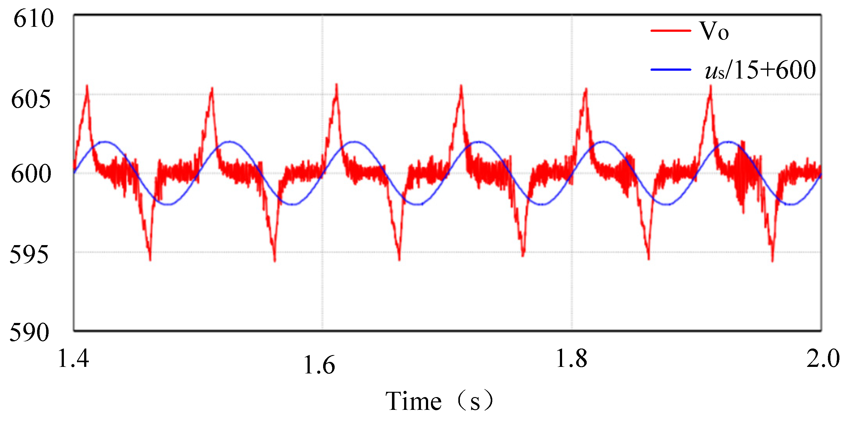
The purpose of the simulation experiment of power disturbance is to compare the ability of DC/DC converter to resist power disturbance under two different control strategies. The output parameters are: DC voltage 750V and superimposed with a disturbance AC voltage with a peak value of 30V and a frequency of 10Hz. The output voltage is set to 600V, the current limit is set to 25A, and the load is set to 30Ω. The simulation waveforms are shown in Figure 19 and Figure 20.
In the above Figures, Vo represents the output voltage waveform, and us represents the superimposed disturbance AC voltage. In order to highlight the contrast effect, the voltage waveform of us is scaled 15 times and translated to 600V. It can be seen from the simulation waveform that the output voltage of the charger converter under the double closed-loop cascade control strategy fluctuates due to the interference of the input disturbance voltage, and the fluctuation amplitude is ±5V, accounting for 16% of the disturbance voltage fluctuation amplitude. The output voltage fluctuation amplitude under the modulation wave selection control strategy of the charger converter is also ±5V, but it can be recovered by rapid adjustment. The simulation results show that the modulation wave selection control strategy has faster voltage regulation speed and stronger anti-power disturbance ability than the traditional double closed-loop cascade control strategy.
5. Conclusions
Based on the analysis of the working principle, circuit design and working loss of the common charger DC/DC converter, this paper introduces a commonly used ZVS half-bridge three-level DC/DC converter based on non-phase-shift control mode, and proposes a multi-stage constant current and voltage-limiting charging control strategy based on modulation wave selection control. Finally, the simulation experiment is carried out. The conclusions are as follows:
(1) The multi-stage constant current and voltage limiting charging control strategy based on modulation wave selective control proposed in this paper can realize the constant voltage and current limiting charging control and module parallel current sharing control which are not available in the traditional double closed-loop cascade control strategy. It is very suitable for the multi-module parallel control system of charger.
(2) Under the same load disturbance, the regulating time of suppressing voltage fluctuation of charger converter under two control strategies has little difference, but the amplitude of output voltage fluctuation under modulation wave selection control strategy is much smaller than that under double closed-loop cascade control strategy.
(3) The modulation wave selection control strategy has faster voltage regulation speed and stronger anti-power disturbance ability than the traditional double closed-loop cascade control strategy, and the dynamic performance is better than the double closed-loop cascade control strategy.
Author Contributions
Conceptualization, H. Shen. and R.Yan.; methodology, H. Shen. and J. Zhou.; software, J. Zhou.; formal analysis, H. Shen.; investigation, H. Shen.; data curation, J. Zhou.; writing—original draft preparation, H. Shen. and L. Pan.; writing—review and editing, L. Pan. and J. Zhou.; All authors have read and agreed to the published version of the manuscript.
Funding
This research was funded by Shanghai Carbon Peak Carbon Neutralization Project ' Research and Application of Intelligent Networked Charging Robot Based on Supercapacitor Energy Storage Technology ', grant number 21DZ1208500.
Institutional Review Board Statement
Not applicable.
Informed Consent Statement
Not applicable.
Data Availability Statement
Not applicable.
Conflicts of Interest
The authors declare no conflict of interest.
References
- Guanlei. Research on fast charging technology of electric vehicle charging pile [J].Electronic production, 2022,30 (08) : 95-97. [CrossRef]
- Shao Anchen.Electric vehicle charging efficiency research and AC charging device design [D].Tianjin Vocational and Technical Normal University, 2022. [CrossRef]
- Naoui Mohamed,Flah Aymen,Ben Hamed Mouna. Inductive charger efficiency under internal and external parameters variation for an electric vehicle in motion[J]. International Journal of Powertrains,2020,8(4). [CrossRef]
- Peter, K. Joseph,Elangovan Devaraj. Design of hybrid forward boost converter for renewable energy powered electric vehicle charging applications[J]. IET Power Electronics,2019,12(8). [CrossRef]
- Qian Siqi. Research and design of electric bus charger [D].Hubei University of Arts and Sciences, 2022. [CrossRef]
- Xiong Zhengyao, He Yongyi. Design of automatic test system for new energy vehicle charger [J].Measurement and test technology, 2022,49 (08) : 61-63. [CrossRef]
- Yao Jin. Discussion on verification device and verification method for non-vehicle charger of electric vehicle [J]. Automation application, 2022 (08): 4-8. [CrossRef]
- Rasool, H.; Verbrugge, B.; Jaman, S.; Abramushkina, E.; Geury, T.; El Baghdadi, M.; Hegazy, O. Design and Real-Time Implementation of a Control System for SiC Off-Board Chargers of Battery Electric Buses. Energies 2022, 15, 1434. [Google Scholar] [CrossRef]
- Xiangwu Yan,Ling Wang,Zhichao Chai,Shuaishuai Zhao,Zisheng Liu,Xuewei Sun. Electric Vehicle Battery Simulation System for Mobile Field Test of Off-Board Charger[J]. Energies,2019,12(15). [CrossRef]
- LI Mingshuo. Research on high power density electric vehicle charger [D]. Nanjing University of Aeronautics and Astronautics, 2015.
- Yao Jun, Zhang Jie, Yao Xiangyu, Dong Qin. Design of high frequency isolated DC charger [J].Electrical applications, 2016, 35, 38–41.
- Zhao Zhen, Liu Yang, Ma Chi, Xie Bingruo, Wang Yongxiang. Dual-phase-shift control of high-frequency isolated DC-DC converters for on-board power electronic transformers [J].Rail vehicles, 2020,40 (06) : 1-5 + 10.
- Shunsuke TAKAHASHI,Kenji SHIBA. Air-core Transcutaneous Energy Transmission System for Ventricular Assist Device with High-frequency Isolation Transformer:[J]. Journal of the Japan Society of Applied Electromagnetics and Mechanics,2019,27(3). [CrossRef]
- Application of AC power supply in vehicle charger test [J]. China Integrated Circuits, 2017, 26 (06): 62-64.
- Li Jingxuan, Lu Yansong, Zhu Chong, Lu Xu, Zhang Xi. Thermal management strategy of electric vehicle fast charging module based on predictive control [J/OL]. Power Journal: 1-10 [2022-12-30].
- Zou Chengyu. Research on Charging Control Method and Current Sharing Strategy of Rear Stage DC/DC Converter of Charger [D]. Xi 'an University of Technology, 2017.
- Power loss analysis and circuit design of DC/DC charger [D].University of Electronic Science and Technology of China, 2016.
- Li Yulan,Wang Guangyan. Research on DC Charger Interoperability Test for Electric Vehicles[J]. Journal of Physics: Conference Series,2021,1754(1). [CrossRef]
- Zhou Zhuo, Lu Xiang, Liu Haitao, Qi Shenglong, Han Tao, Wang Qing. Research on online optimization strategy of charging power of electric vehicle charging station with new energy generation [J/OL].Electrical measurement and instrument: 1-8 [2022-11-01].
- Research on a five-level DC-DC charging module [D].Beijing Jiaotong University, 2021. [CrossRef]
- Shi Wenye, He Zhiqin, Zhu Youtao. Research on control strategy of three-phase AC / DC bidirectional converter for charging pile [J].Automotive technology, 2022 (06) : 33-39. [CrossRef]
- Tao Haijun, Qin Xidong, Zheng Zheng. Research on DC / DC converter for electric vehicle charging [J]. Journal of Nanjing University of Science and Technology, 2019,43 (03): 312-319. [CrossRef]
Figure 1.
Power supply framework of vehicle charger.
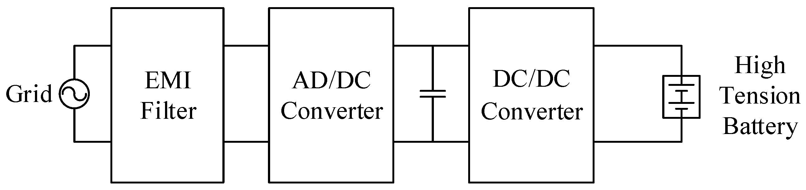
Figure 2.
Hard switch working process.
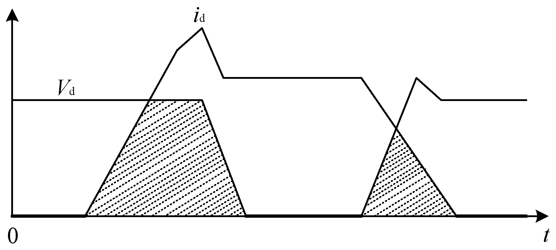
Figure 3.
Working process of soft switch.
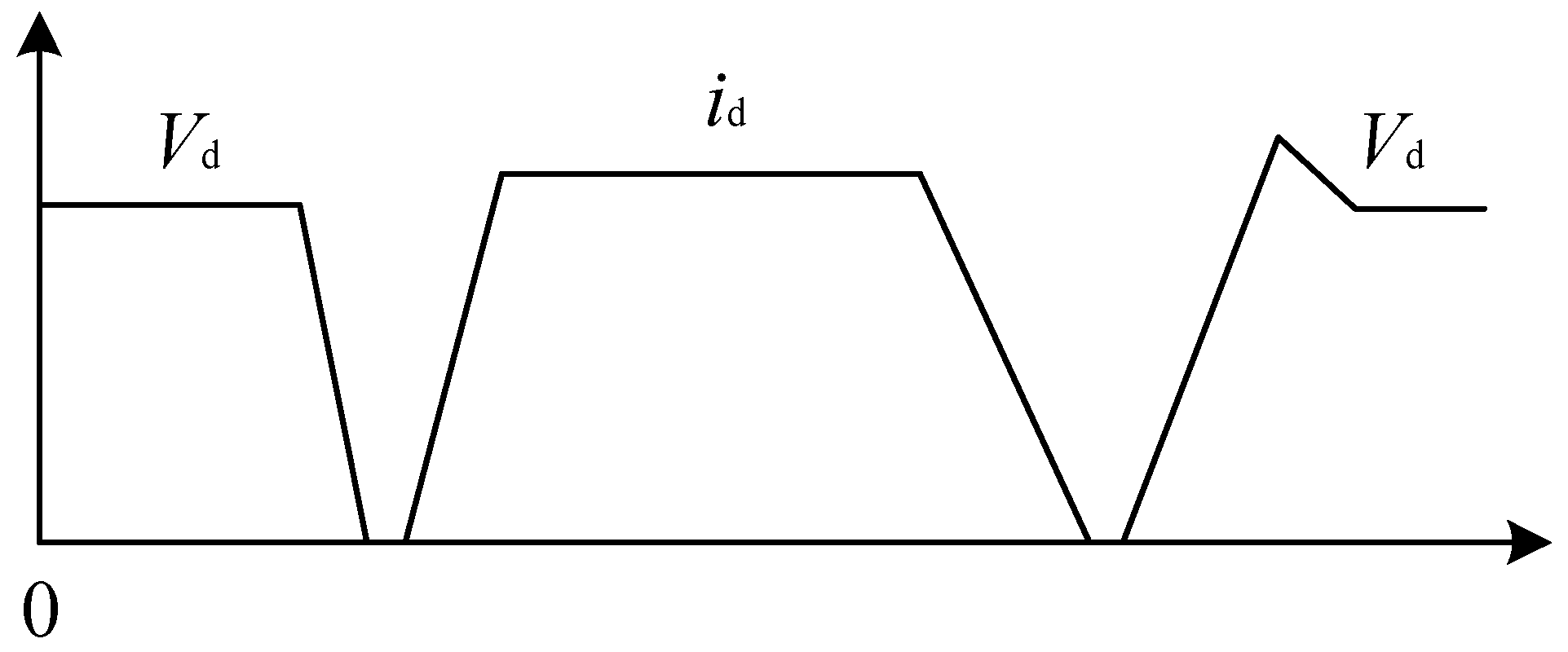
Figure 4.
ZVS half-bridge three-level DC/DC converter topology.
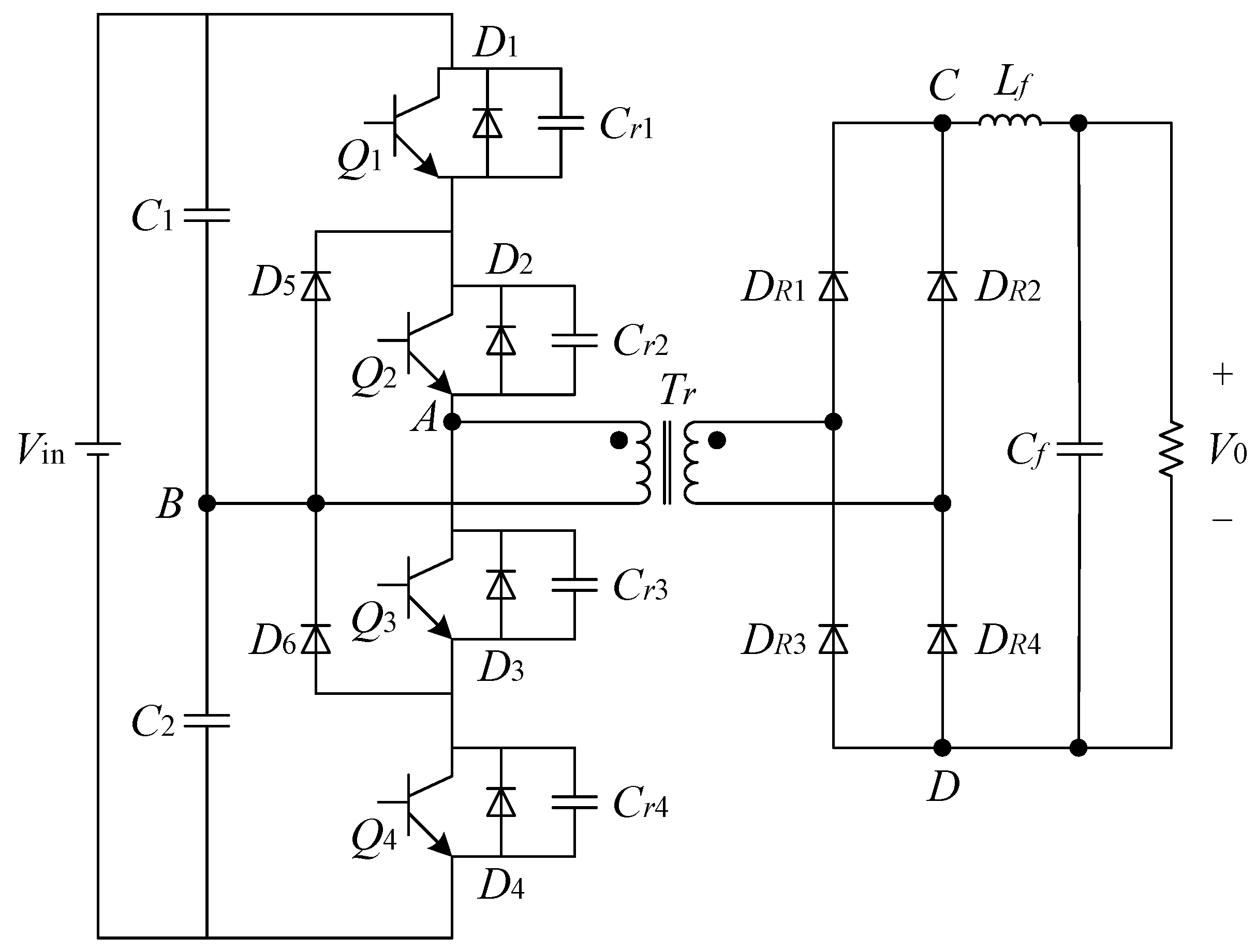
Figure 5.
Basic PWM control mode of ZVS half-bridge three-level DC / DC converter.
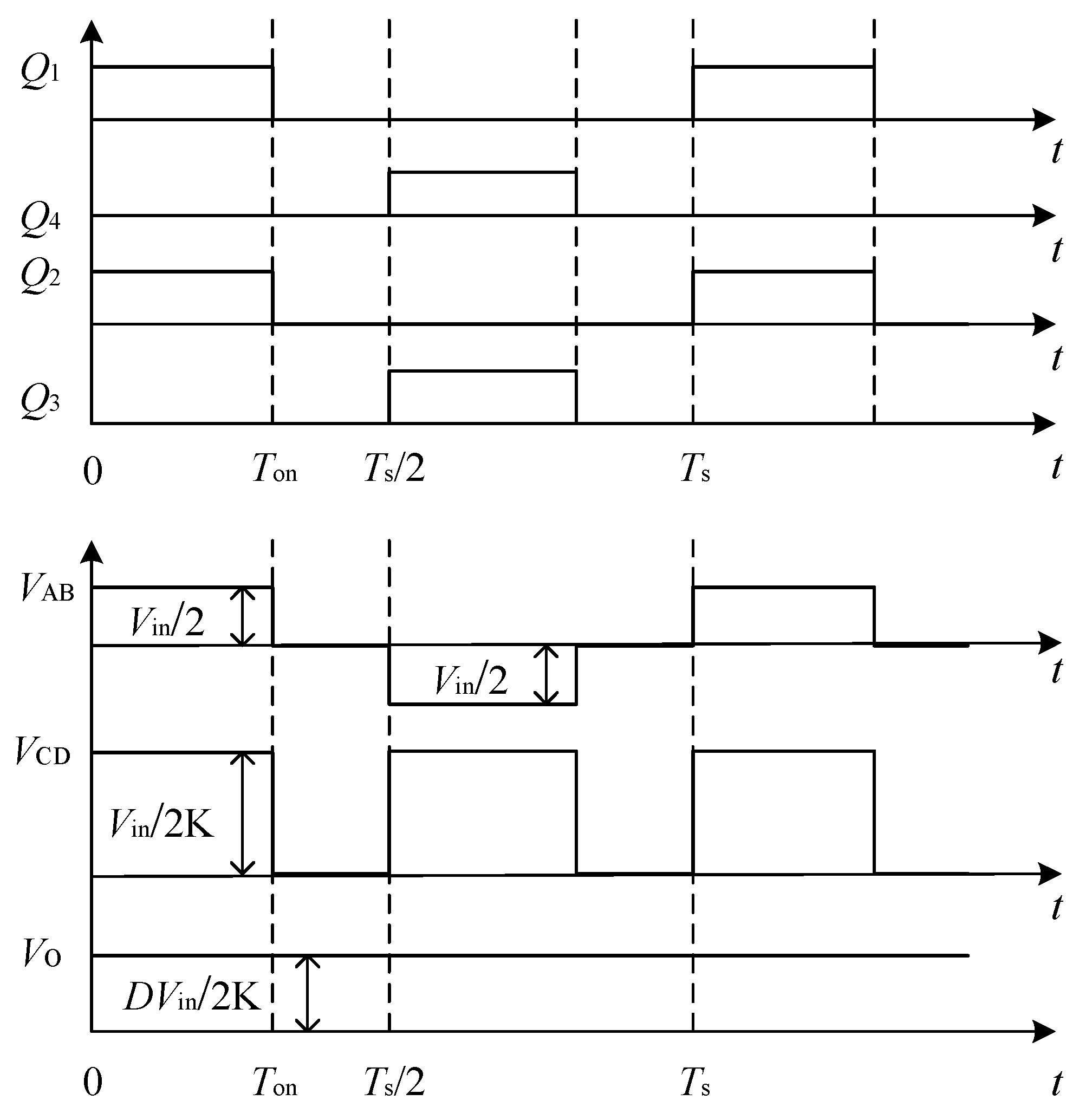
Figure 6.
Four PWM control methods of ZVS half-bridge three-level DC/DC converter.
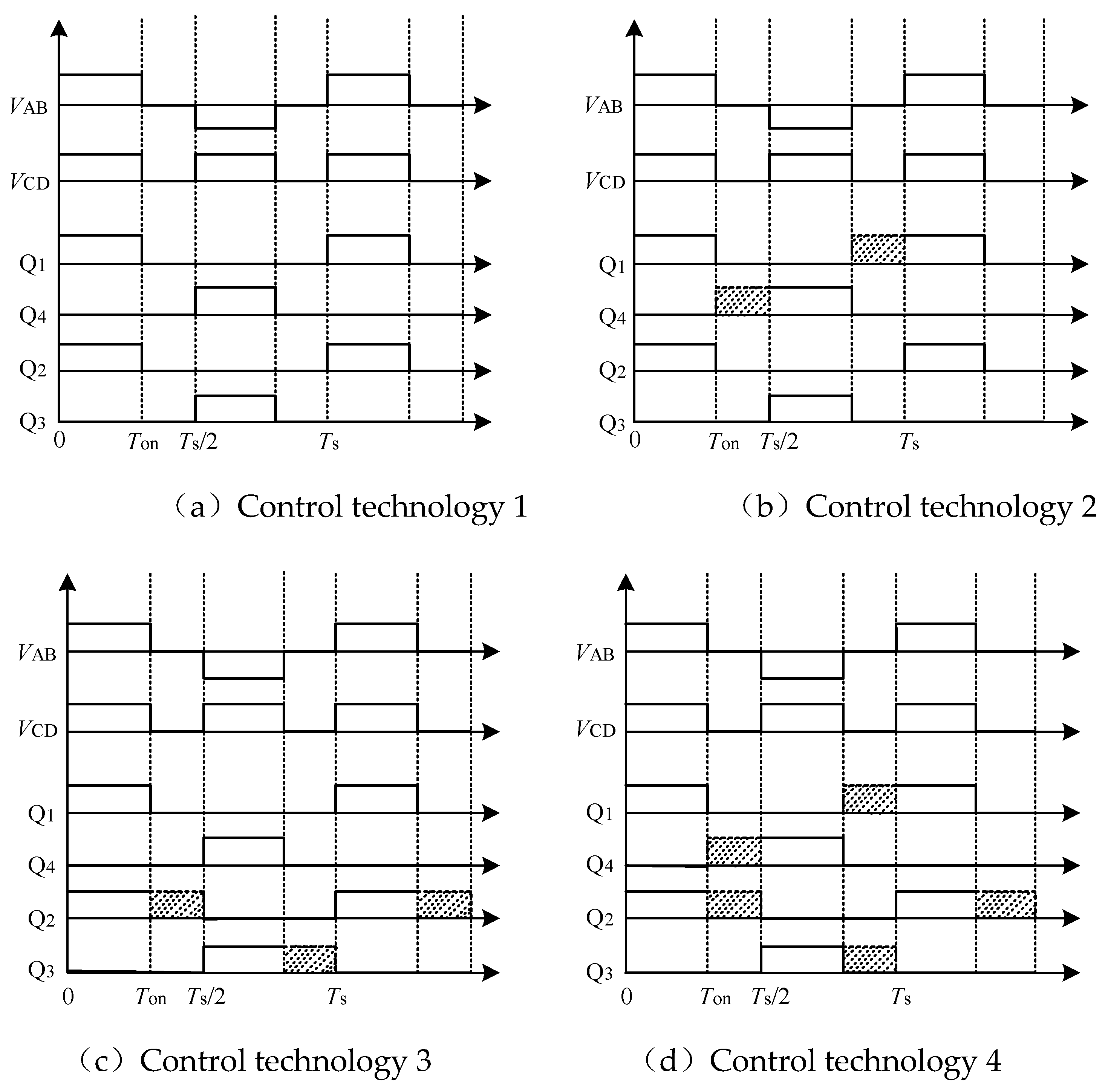
Figure 7.
Mas charging curve.
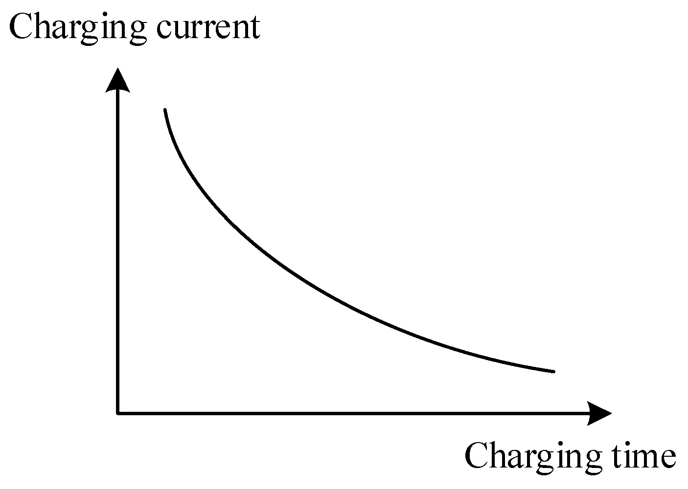
Figure 8.
Double closed-loop cascade control system block diagram.
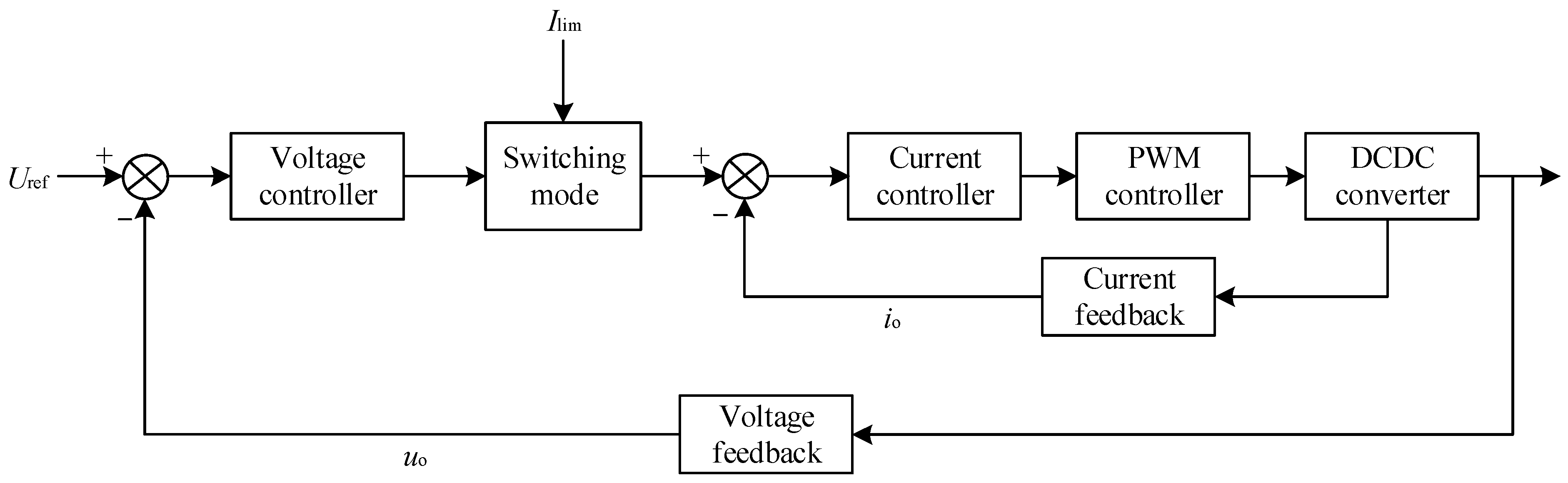
Figure 9.
Principle Diagram of Double Closed Loop Cascade Control Strategy.
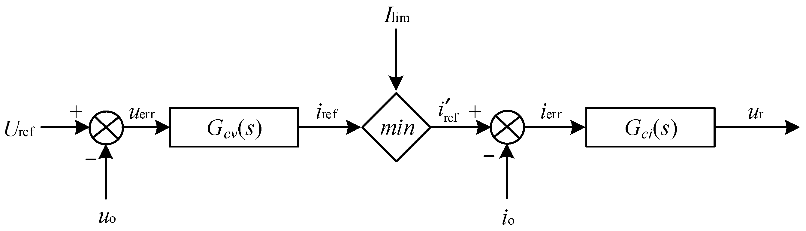
Figure 10.
Modulation wave selection control system block diagram.
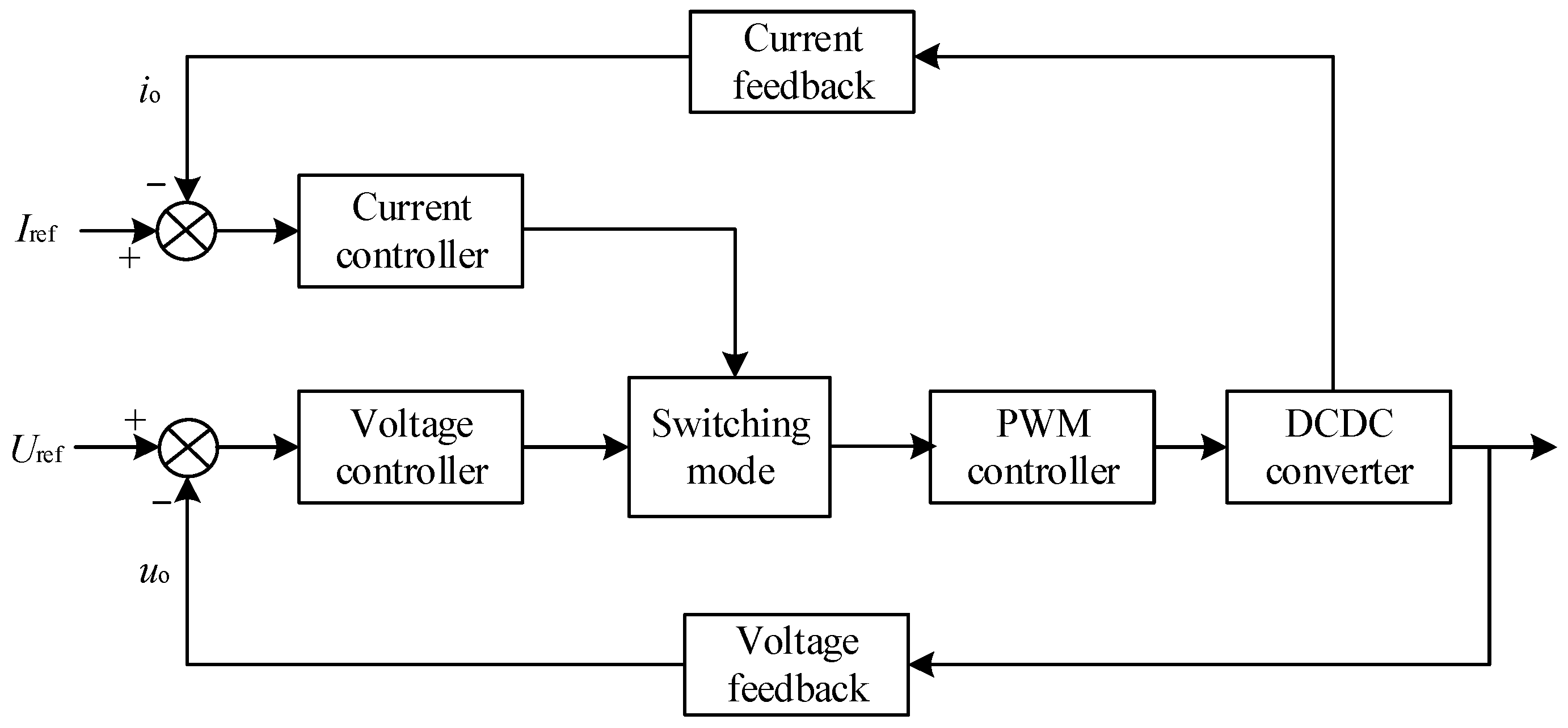
Figure 11.
Modulation wave selection control strategy principle flow chart.
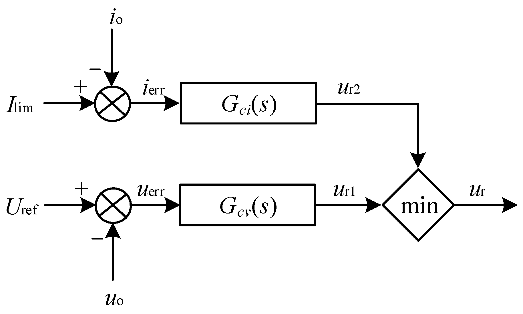
Figure 12.
Simulation model of charger DC/DC converter.
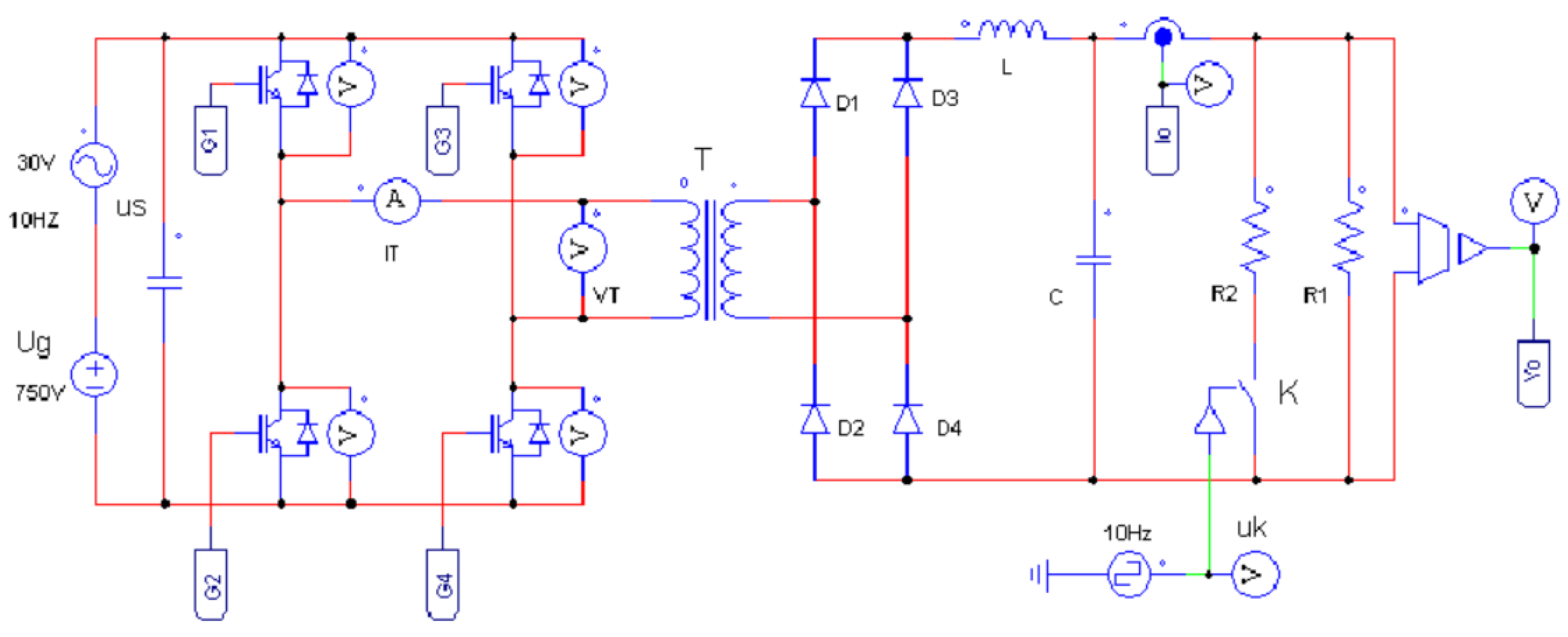
Figure 13.
Double closed-loop cascade control circuit.
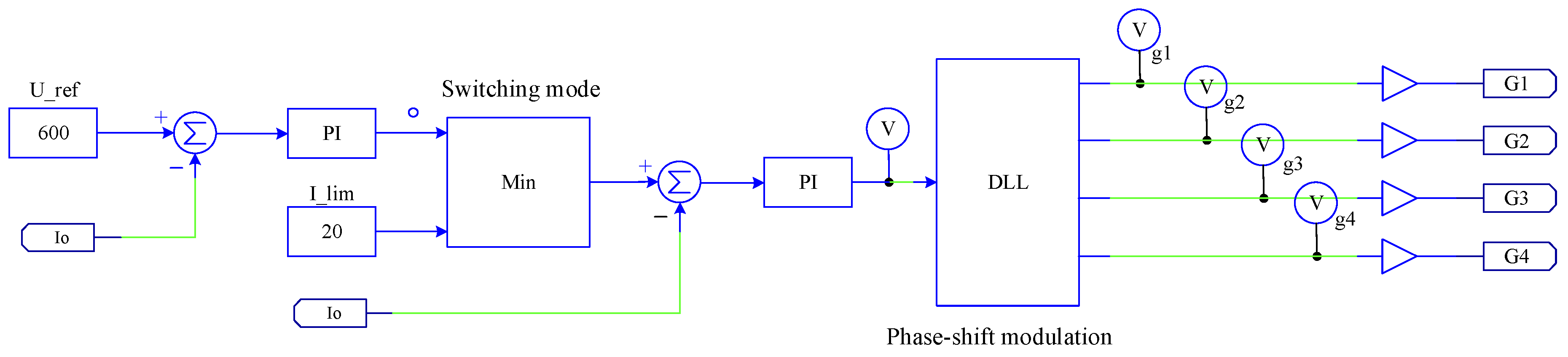
Figure 14.
Modulation wave selection control circuit.
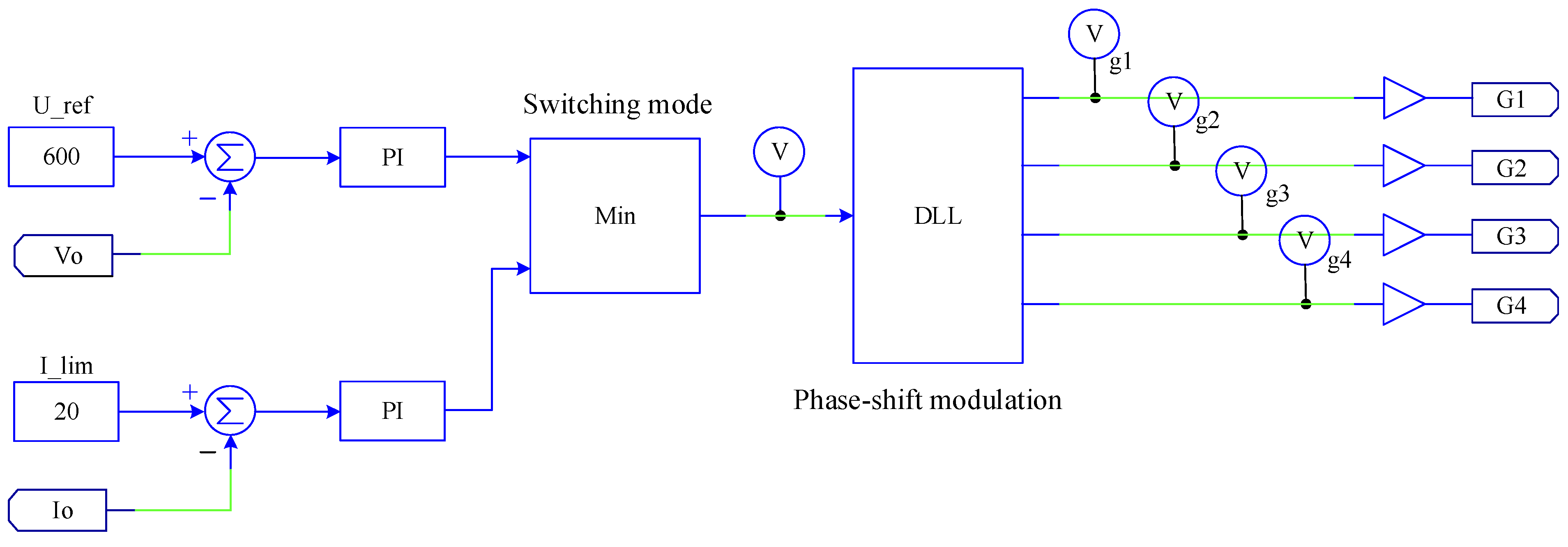
Figure 15.
Double closed-loop cascade control strategy simulation waveform.
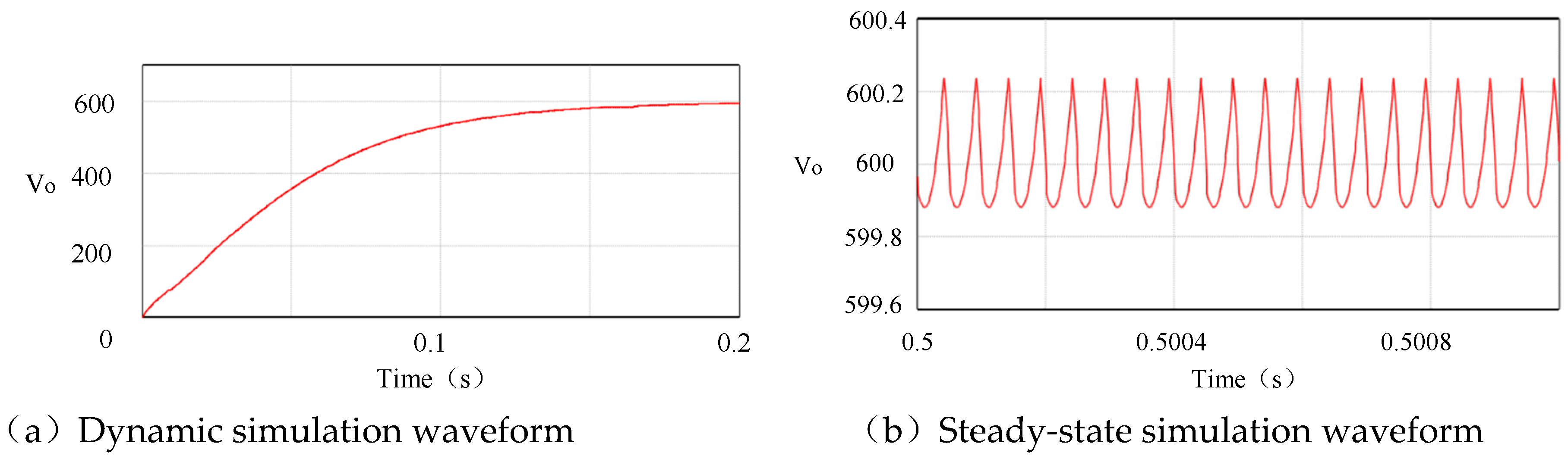
Figure 16.
Modulation wave selection control strategy simulation waveform.
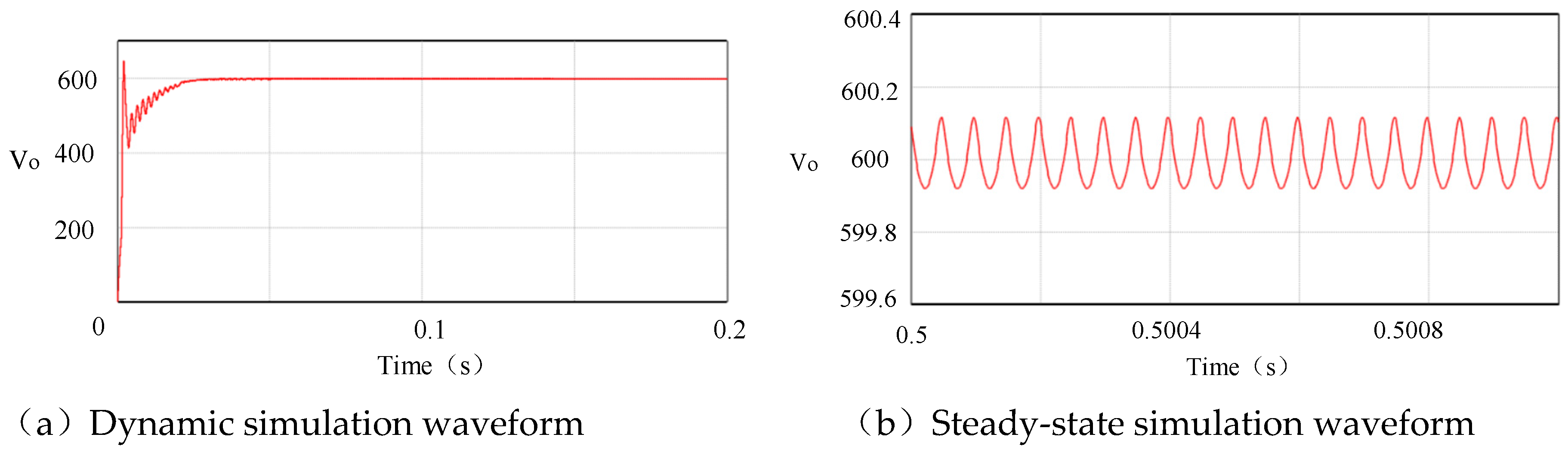
Figure 17.
Double closed-loop cascade control strategy load disturbance simulation waveform.
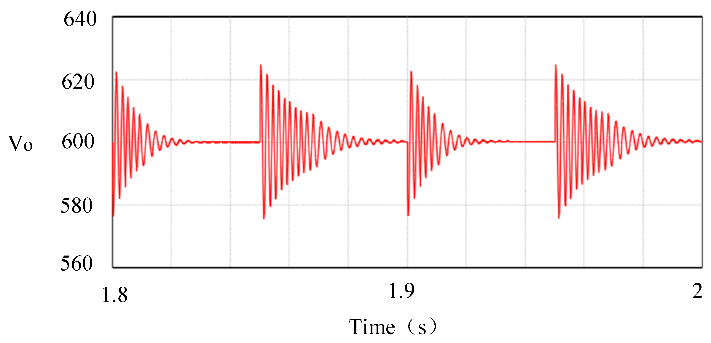
Figure 18.
Modulation Wave Selection Control Strategy Load Disturbance Simulation Waveform.
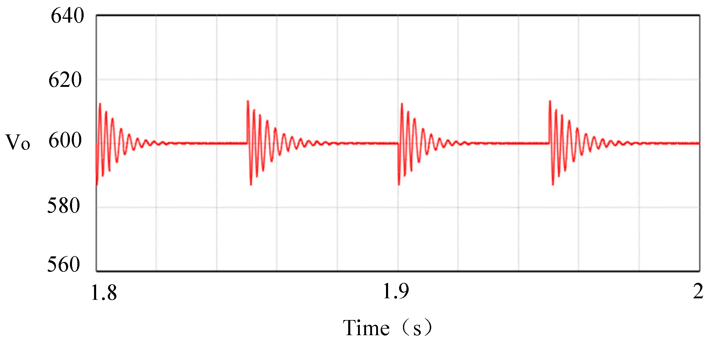
Figure 19.
Double closed-loop cascade control strategy DC power supply disturbance simulation.
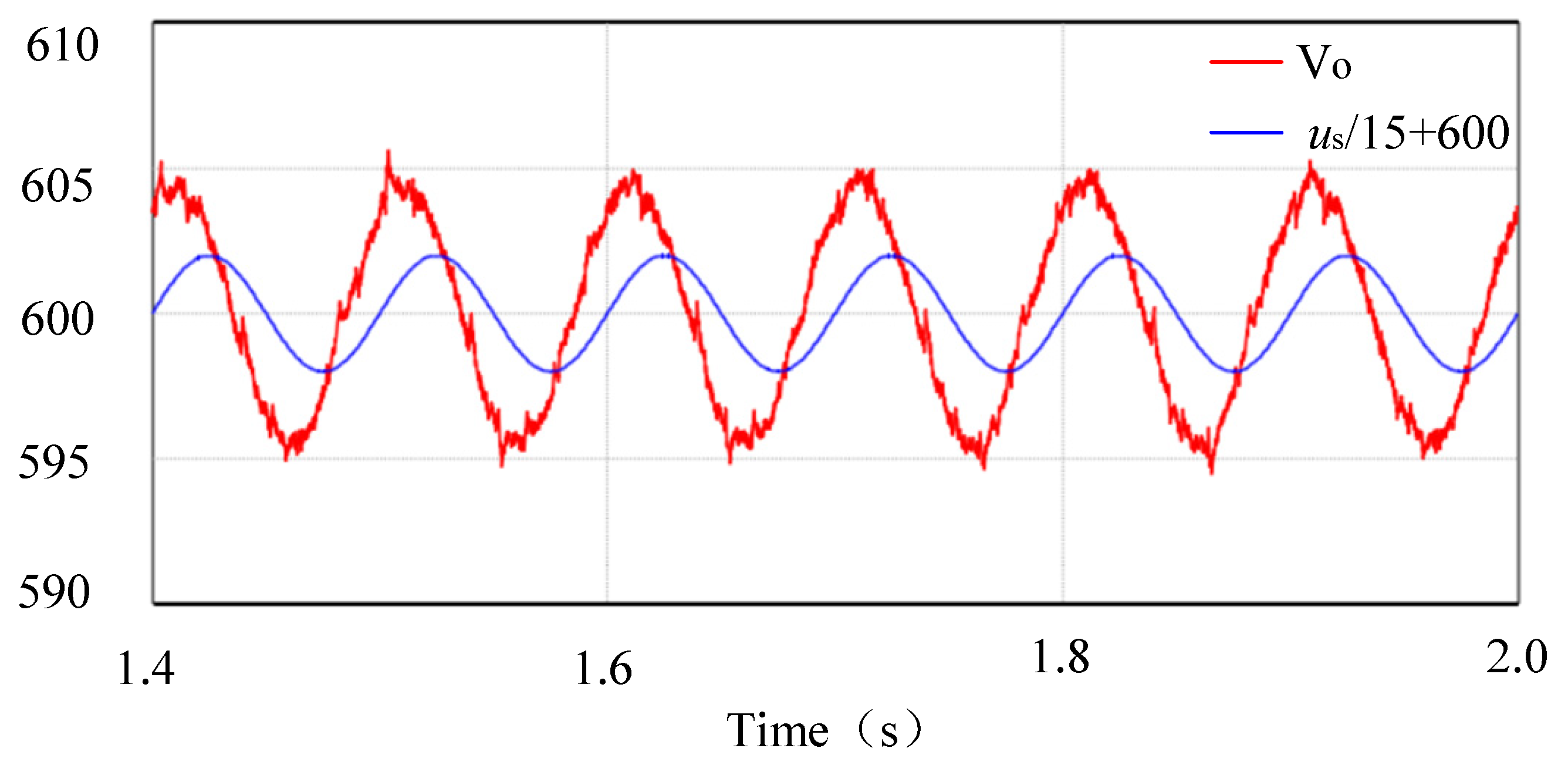
Figure 20.
Modulation wave selection control strategy DC power disturbance simulation.
Disclaimer/Publisher’s Note: The statements, opinions and data contained in all publications are solely those of the individual author(s) and contributor(s) and not of MDPI and/or the editor(s). MDPI and/or the editor(s) disclaim responsibility for any injury to people or property resulting from any ideas, methods, instructions or products referred to in the content. |
© 2023 by the authors. Licensee MDPI, Basel, Switzerland. This article is an open access article distributed under the terms and conditions of the Creative Commons Attribution (CC BY) license (http://creativecommons.org/licenses/by/4.0/).
Copyright: This open access article is published under a Creative Commons CC BY 4.0 license, which permit the free download, distribution, and reuse, provided that the author and preprint are cited in any reuse.


