
Submitted:
16 October 2023
Posted:
19 October 2023
You are already at the latest version
Abstract
Although hundreds of keV in energy gain have already been demonstrated in dielectric laser accelerators (DLAs), there remains challenge in creating structures that can confine electrons for multiple millimeters. We focus here on dual gratings with single sided drive, which have experimentally demonstrated energy modulation numerous times. Using a FTDT simulation to find the fields within various DLA structures and correlating these results with particle tracking simulation, we look at the impact of teeth height and width, as well as gap and offset, on the performance of these structures. We find a tradeoff between electron throughput and acceleration, but that for any given grating geometry there is a gap and offset that will allow some charge acceleration. For our 780 nm laser wavelength, this results in a 1200 nm optimal gap size for most gratings.
Keywords:
DLA
; Dielectric Laser Accelerator
; Dual Grating
; Single Drive
1. Introduction
Dielectric laser accelerators could allow for the proliferation of accelerator devices throughout small laboratory and medical settings. Enabled by materials advancement and power efficient laser technology, DLAs have produced GeV/m gradients and >700 m interaction lengths [1,2]. However, energy gain has been limited to 300 keV, in part by the difficulty of manufacturing long structures with sub-micron gap sizes. Many structures have been proposed, but dual grating structures remain useful for their simplicity and tunability [3,4].
Prior optimization works have limited themselves primarily to gaps less than the illumination wavelength, [5,6,7,8,9]. However, for experimental demonstrations of long interactions there is a major reason one might want to increase that gap size - charge throughput. In addition, there remain challenges with the manufacture of bonded structures of multi-mm scale, which prohibits the setting of one particular gap size. Instead, a mounting scheme for dual gratings has been developed which allows for far more flexibility in structure parameters, even during experiment [10]. This drives the analysis of structures with gratings aligned to non-zero offsets and larger than wavelength gap size.
In this paper, we will first examine the field structure within a standard single drive dual grating structure. Combining this with particle tracking simulations will allow us to determine goal parameters. Thus, we approach the problem of grating geometry sequentially; first by finding the highest efficiency geometry for the grating far from the incident laser (i.e. the right grating), and then scanning over geometries for the left grating. The tradeoff between acceleration and throughput will be discussed in detail, as it drives the optimization of structure parameters. By changing the gap and offset of the structure, we will analyse the expected energy gain and electron throughput of the designed double grating structure.
2. Materials and Methods
We begin by examining the field structure created in the single drive dual grating structure geometry, shown in Figure 1. The laser propagates in the y-direction, polarized parallel to the propagation of the electrons (z). The x-direction is assumed to be semi-infinite such that laser excites a TM mode in the structure. One can describe the order mode in a DLA by the real part of
The laser has angular frequency and amplitude . The coefficients and are complex and describe the amplitude of the waves propagating from the left and right, respectively. Since the laser propagates orthogonal to the structure, there is no additional wavenumber in the beam direction () component. Each must satisfy the dispersion relation
In order to satisfy the phase resonant condition for acceleration , this relation implies the fields of interest are evanescent with decay length , which directs gap sizes to be on the order of a laser wavelength. As the only free parameters in equation 1, and alone may be used to parameterize the DLA. However, it is useful to define some additional quantities to understand accelerating and deflecting modes. As in Dylan et al. [11] we define the parameter as
It can be useful to think not only in terms of , but instead in terms of the location of the potential minimum in the structure, , labeled in Figure 2. We calculate the location of the minimum of to be and define the effective gap as twice the distance from to the nearing grating wall. Finally, we define the structure factor
and note that this definition agrees with prior definitions where the accelerating gradient is equal to when the phase velocity of the mode is matched to the electron velocity.
When the relative amplitudes of the counterpropagating waves are equal, as would be the case in a symmetric dual illuminated structure, and . In this case, when the relative phase a symmetric accelerating cosh-like mode is formed around the center of the gap. Conversely, when a deflecting sinh mode is created. Since our focus is in creating accelerators with high accelerating gradients and high throughput, it is clear that must be kept close to 0 in order to avoid deflecting the majority of electrons.
To better quantify this, we measure throughput of particles in a toy structure using a spatial harmonics based simulation (SHarD), which is explained at length by Ody et al. [12]. For the illumination we assume a Gaussian laser pulse with peak field of 1 GV/m and of 5 mm to be incident on a 5 mm, 780 nm periodicity structure with an 800 nm gap. 1000 electrons are initialized with 6 MeV energy, 0.1 nm emittance and are uniformly spaced within a grating period. The laser field phase is tapered to match the energy gain of the accelerated electrons, there is no Alternating Phase Focusing [13,14] or ponderomotive based focusing [15] scheme. Without incident field, 99.3% of particles are transmitted; this drops to 57.2% with the addition of an input field. Since the particles are initially unbunched, many lose energy throughout the structure. We therefore define a ’captured’ particle to be one with , and use this as the figure of merit.
Figure 3 shows the result of varying r and in this toy structure while keeping the structure factor constant. In the absence of a single drive constraint, one can see a very clear design target - symmetry, with and . However, implementing a single sided drive (and dual grating) means one must instead balance capture rates with structure factor. From the toy model we gather that at the least, must be located within the structure gap (), and kept to below radians.
From here, we assert that the ideal accelerating structure would have maximal structure factor, maximal effective gap, and close to zero. Because it is not possible to both maximize and minimize and , we instead seek to understand the relation between structure geometries and these parameters such that an adequate middle ground is reached.
3. Results
The FTDT simulation software Lumerical is used in order to simulate fields within the grating structures. A plane wave source is injected orthogonal to the DLA structure. The teeth are defined with a 10deg taper, in accordance with etching capabilities (although this does not significantly affect parameters). Upon transmission through the structure, a perfectly matched layer (PML) eliminates extraneous reflections in y. The structure is assumed perfectly periodic (and infinite) in z, so a periodic boundary condition is used. Fused silica with a refractive index of 1.45 is used, due to its high damage threshold and commercial availability.
A frequency domain monitor is used to retrieve the electric field throughout the structure gap and Fourier transformed to phase velocity match a 6 MeV electron. We can fit to equation 1 using as shown in the Figure 2 example.
Although the fields are defined by only and , they are controlled by a number of input parameters. For these dual grating structures, the teeth height, teeth width, gap, and offset are all controllable parameters. Of these, teeth height and teeth width are intrinsic to the manufactured grating; gap and offset can in principle be controlled in assembly. To verify our simulations, we inputted the parameters for the Peralta structure and found a structure factor of 0.24, in agreement with previous calculations [2,6].
For initial simulations, the gratings on top and bottom were identical - we will refer to these as symmetric structures, regardless of offset. The gap size is 800 nm; smaller gaps result in very low transmission, which make them unrealistic target structures for near-term experiments. The tooth width is set to a 50 % duty cycle, 390 nm. Then tooth height was scanned over from 300 nm to 900 nm. Figure 4 shows the results of this scan; the maximum at 650 nm in tooth height shows the best geometry for the right grating. Following this, a scan over tooth width from 200 nm to 600 nm was done, again with symmetric structures (with teeth height set to 650 nm); the optimal width is 425 nm, or 54% duty cycle.
From these scans, a baseline optimal grating for maximal structure factor is found. As was previously discussed, however, this analysis ignores the very significant impact of asymmetric fields within the structure for the single drive case. We therefore move on to structures with asymmetric tooth height.
It is informative to look at the how gap and offset impact the retrieved and r. Figure 5 shows this relation for the structure with a left tooth height of 450 nm. It is seen that both in gap and offset there is a periodicity in phase. For these gratings, gaps larger than 800 nm allow for to be close to zero. Due to the deflecting forces for nonzero , this means that shrinking the gap size to optimize structure factor would be ineffective in improving the DLA.
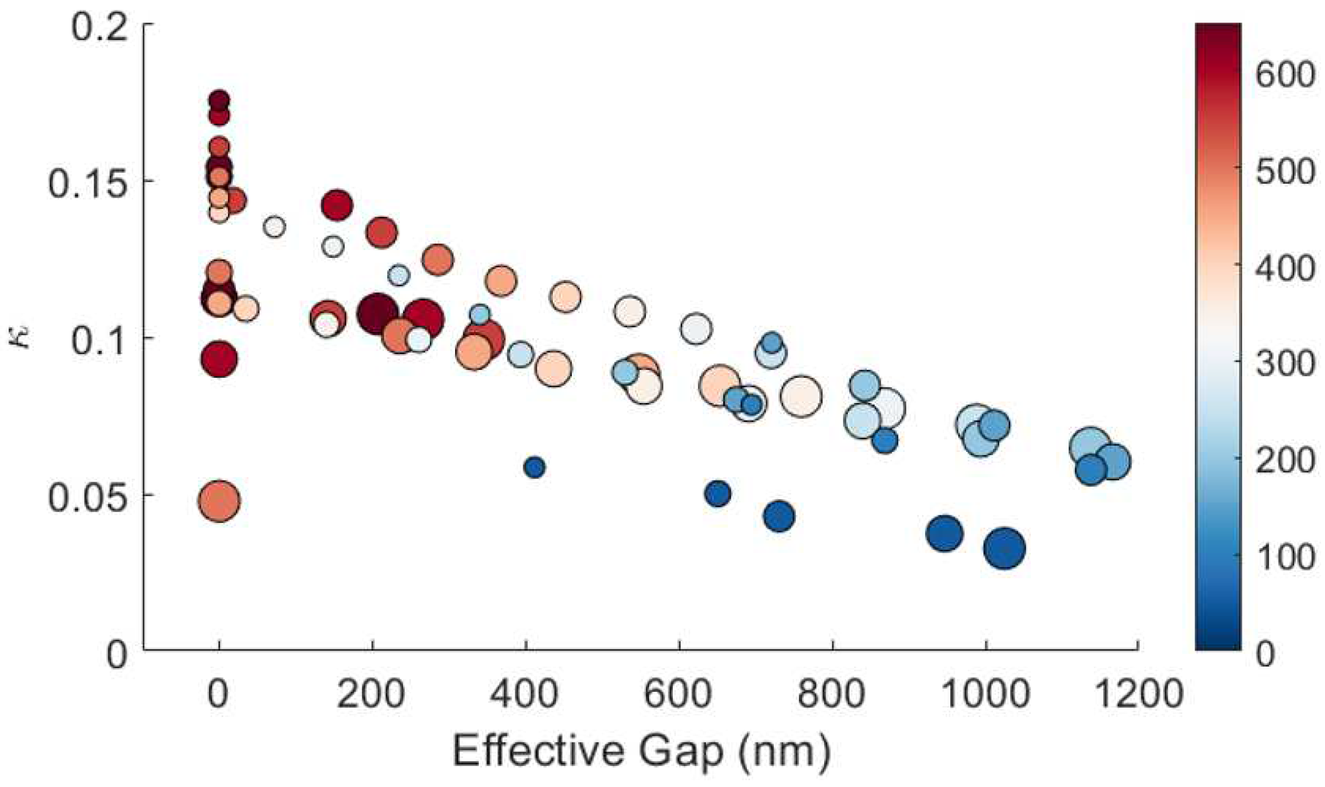
Seeking to find the optimal combination of asymmetric grating geometries, we do an additional parameter scan. The right grating is set with 425 nm tooth width and 650 nm tooth width. We then vary the left grating tooth height, while letting the offset and gap size change. Because is critical to minimizing the sinh deflection mode, in Figure 6 we plot only the gap-offset combinations which minimize , and the resulting upper right boundary is the Pareto front. We are using effective gap here as a proxy for particle capture, although there is certainly interplay between the acceptance space of and .
The darkest blue points correspond to 50 nm teeth; the structure factor is lowest due to the inefficiency of the left grating, and is moved so far to the left that the effective gap is lower than structures with higher . For the symmetric structure (650 nm) only the 1600 nm gap has an effective gap larger than 0 nm. However, this lands the structure well under the Pareto front. In fact, it appears that the Pareto front is mostly composed of 1200 nm gap structures. Further study would be needed to find the proportionality of this to structure periodicity.
4. Discussion
We conclude that for our 780 nm, single side illuminated, dual grating structure, the optimal gap size is 1200 nm, far from the criterion which maximizes . If all possible gap sizes and offsets are available (as in general they are when using slab gratings), any tooth height could give rise to an effective gap larger than zero as well while having a near zero .
In summary, we have examined the optimization for a single drive dual grating structure. We find that by varying the teeth height and width of the gratings we may modify the peak structure factor and effective gap. We find that only a small subset of gap and offset combinations will minimize the relative phase which is required for an accelerating mode. In fact, not all grating geometries allow for the minimization of at all, at least when restricted to gaps on the order of the laser wavelength.
This analysis is critical for understanding the expected accelerated population from a given DLA. Since sub-micron gap sizes inherently limit charge throughput, care must be taken to assemble structures with a balance between acceleration gradient and effective gap. Using simple unchirped gratings like these reduces cost while allowing for soft-tuning approaches like laser phase tapering to address dynamic effects from longer interactions [16].
Author Contributions
Conceptualization, P.M. and S.C.; methodology, A.O. and S.C.; software, S.C. and A.O.; validation, S.C. and A.O.; formal analysis, S.C.; investigation, S.C.; resources, P.M.; data curation, S.C. and A.O.; writing—original draft preparation, S.C.; writing—review and editing, S.C., A.O. and P.M.; visualization, S.C.; supervision, P.M.; project administration, P.M.; funding acquisition, P.M. All authors have read and agreed to the published version of the manuscript.
Funding
This work has been supported by the ACHIP grant from the Gordon and Betty Moore Foundation (GBMF4744) and by U.S. Department of Energy Grant No. DE-AC02-76SF00515. This material is based upon work supported by the National Science Foundation Graduate Research Fellowship Program under Grant No. DGE-1650604. Any opinions, findings, and conclusions or recommendations expressed in this material are those of the author(s) and do not necessarily reflect the views of the National Science Foundation.
Data Availability Statement
The data presented in this study are available on request from the corresponding author.
Acknowledgments
Thanks to Kristian Buchwald at Ibsen Photonics for support in looking at realistic grating parameters.
Conflicts of Interest
The authors declare no conflict of interest.
References
- Cesar, D.; Maxson, J.; Shen, X.; Wootton, K.P.; Tan, S.; England, R.J.; Musumeci, P. Enhanced energy gain in a dielectric laser accelerator using a tilted pulse front laser. Opt. Express 2018, 26, 29216–29224. [Google Scholar] [CrossRef] [PubMed]
- Cesar, D.; Custodio, S.; Maxson, J.; Musumeci, P.; Shen, X.; Threlkeld, E.; England, R.J.; Hanuka, A.; Makasyuk, I.V.; Peralta, E.A.; et al. High-field nonlinear optical response and phase control in a dielectric laser accelerator. Communications Physics 2018 1:1 2018, 1, 1–7. [Google Scholar] [CrossRef]
- England, R.J.; Noble, R.J.; Bane, K.; Dowell, D.H.; Ng, C.K.; Spencer, J.E.; Tantawi, S.; Wu, Z.; Byer, R.L.; Peralta, E.; et al. Dielectric laser accelerators. Rev. Mod. Phys. 2014, 86, 1337–1389. [Google Scholar] [CrossRef]
- Crisp, S.; Ody, A.; Musumeci, P.; England, R.J. Resonant phase matching by oblique illumination of a dielectric laser accelerator. Physical Review Accelerators and Beams 2021, 24. [Google Scholar] [CrossRef]
- Plettner, T.; Lu, P.P.; Byer, R.L. Proposed few-optical cycle laser-driven particle accelerator structure. Phys. Rev. ST Accel. Beams 2006, 9, 111301. [Google Scholar] [CrossRef]
- Peralta, E.A.; Colby, E.; England, R.J.; McGuinness, C.; Montazeri, B.; Soong, K.; Wu, Z.; Byer, R.L. Design, fabrication, and testing of a fused-silica dual-layer grating structure for direct laser acceleration of electrons. AIP Conference Proceedings 2012, 1507, 169–177. [Google Scholar] [CrossRef]
- Aimidula, A.; Bake, M.A.; Wan, F.; Xie, B.S.; Welsch, C.P.; Xia, G.; Mete, O.; Uesaka, M.; Matsumura, Y.; Yoshida, M.; et al. Numerically optimized structures for dielectric asymmetric dual-grating laser accelerators. Physics of Plasmas 2014, 21, 023110. [Google Scholar] [CrossRef]
- Wei, Y.; Ibison, M.; Xia, G.; Smith, J.D.A.; Welsch, C.P. Dual-grating dielectric accelerators driven by a pulse-front-tilted laser. Appl. Opt. 2017, 56, 8201–8206. [Google Scholar] [CrossRef] [PubMed]
- Wei, Y.; Jamison, S.; Xia, G.; Hanahoe, K.; Li, Y.; Smith, J.D.A.; Welsch, C.P. Beam quality study for a grating-based dielectric laser-driven accelerator. Physics of Plasmas 2017, 24, 023102. [Google Scholar] [CrossRef]
- Crisp, S.; Ody, A.; Musumeci, P. All Optical Chartacterization of a Dual Grating Accelerator Structure 2022. https://doi.org/10.18429/JACoW-IPAC2022-WEOXSP2.
- Black, D.S.; Zhao, Z.; Leedle, K.J.; Miao, Y.; Byer, R.L.; Fan, S.; Solgaard, O. Operating modes of dual-grating dielectric laser accelerators. Physical Review Accelerators and Beams 2020, 23. [Google Scholar] [CrossRef]
- Ody, A.; Crisp, S.; Musumeci, P.; Cesar, D.; England, R.J. SHarD: A beam dynamics simulation code for dielectric laser accelerators based on spatial harmonic field expansion. Nuclear Instruments and Methods in Physics Research Section A: Accelerators, Spectrometers, Detectors and Associated Equipment 2021, 1013, 165635. [Google Scholar] [CrossRef]
- Niedermayer, U.; Egenolf, T.; Boine-Frankenheim, O.; Hommelhoff, P. Alternating-Phase Focusing for Dielectric-Laser Acceleration. Phys. Rev. Lett. 2018, 121, 214801. [Google Scholar] [CrossRef] [PubMed]
- Niedermayer, U.; Egenolf, T.; Boine-Frankenheim, O. Three Dimensional Alternating-Phase Focusing for Dielectric-Laser Electron Accelerators. Phys. Rev. Lett. 2020, 125, 164801. [Google Scholar] [CrossRef] [PubMed]
- Naranjo, B.; Valloni, A.; Putterman, S.; Rosenzweig, J.B. Stable Charged-Particle Acceleration and Focusing in a Laser Accelerator Using Spatial Harmonics. Phys. Rev. Lett. 2012, 109, 164803. [Google Scholar] [CrossRef] [PubMed]
- Shiloh, R.; Schönenberger, N.; Adiv, Y.; Ruimy, R.; Karnieli, A.; Hughes, T.; England, R.J.; Leedle, K.J.; Black, D.S.; Zhao, Z.; et al. Miniature light-driven nanophotonic electron acceleration and control. Adv. Opt. Photon. 2022, 14, 862–932. [Google Scholar] [CrossRef]
Figure 1.
Dual grating simulation setup in Lumerical. The source is a 780 nm plane wave at normal incidence, originating from within the structure, since reflection at the surface will be unchanged for each structure. The simulation substrate is 3 m thick; increasing this thickness does not change simulation outputs. The interior orange section is meshed with a 5 nm step. A power monitor records the electric and magnetic fields. The teeth are tapered to reflect realistic etching capabilities.
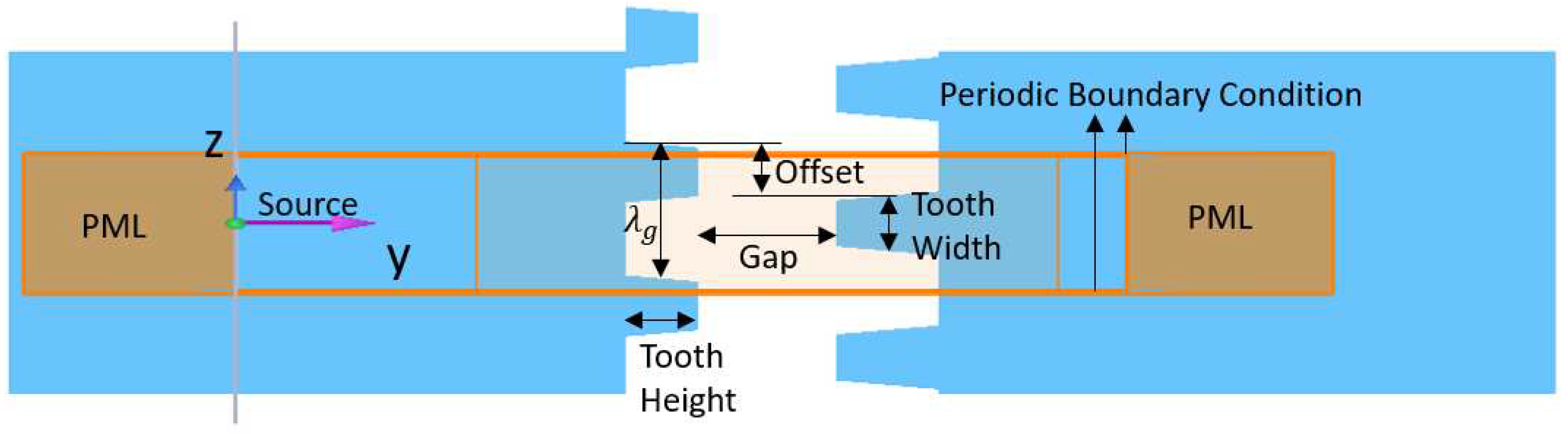
Figure 2.
At left, an example of the average phase matched field from Lumerical and the retrieved fit for a structure with 800 nm gap, left tooth height of 150 nm, right tooth height of 650 nm, and 390 nm tooth width. The offset here was -300 nm to maximize the effective gap. At right, the percent error is shown as a function of gap size. For gaps under 1600 nm, the fitted and match the actual fields curvature to within 0.1 % error.
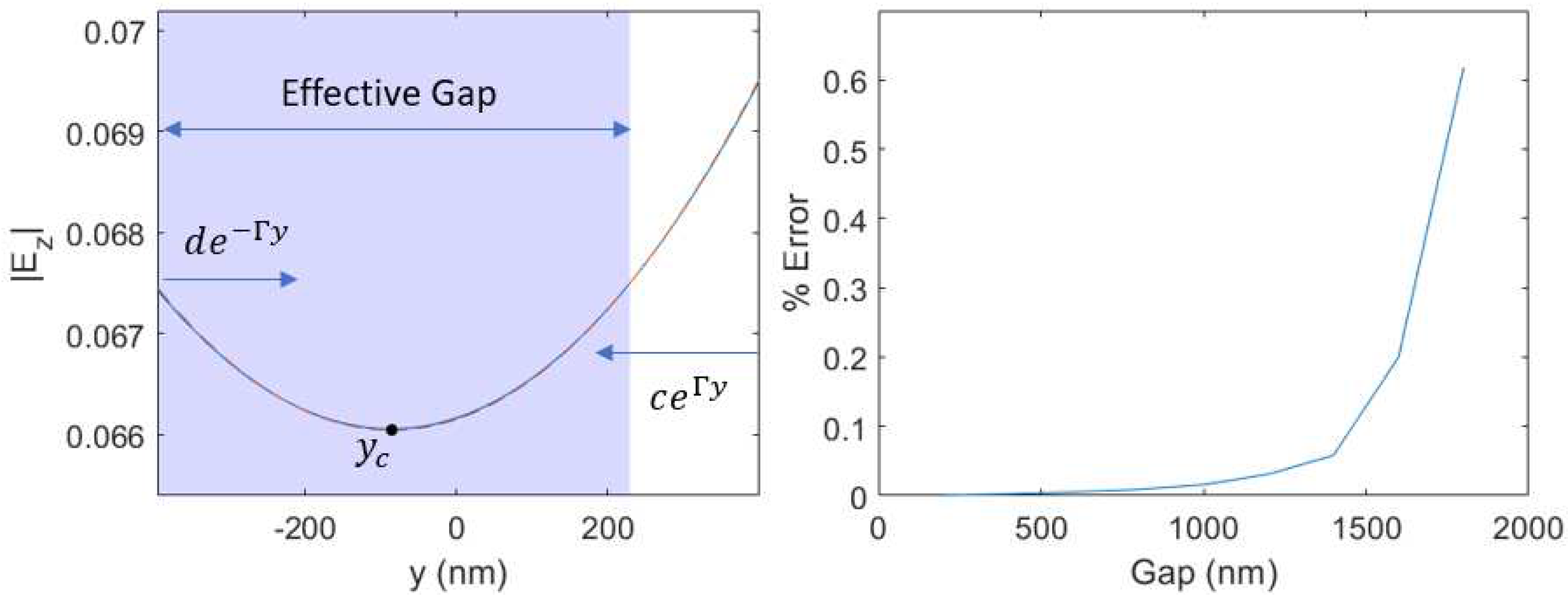
Figure 3.
Simulations with dummy parameters show that less symmetric structures capture fewer particles. These 5 mm long structures have an 800 nm gap and . At left, r is kept at 1 and varied. At right, and r, varied, which equates to moving across the structure gap. Highlighted in purple are the parameters for which >50% of the symmetric case capture rate is obtained. The pink extension refers to structures for which the effective gap is greater than 0 nm, but the capture does not meet the 50% threshold. We conclude that for effective capture, must be within the physical gap, and must be less than 0.2.
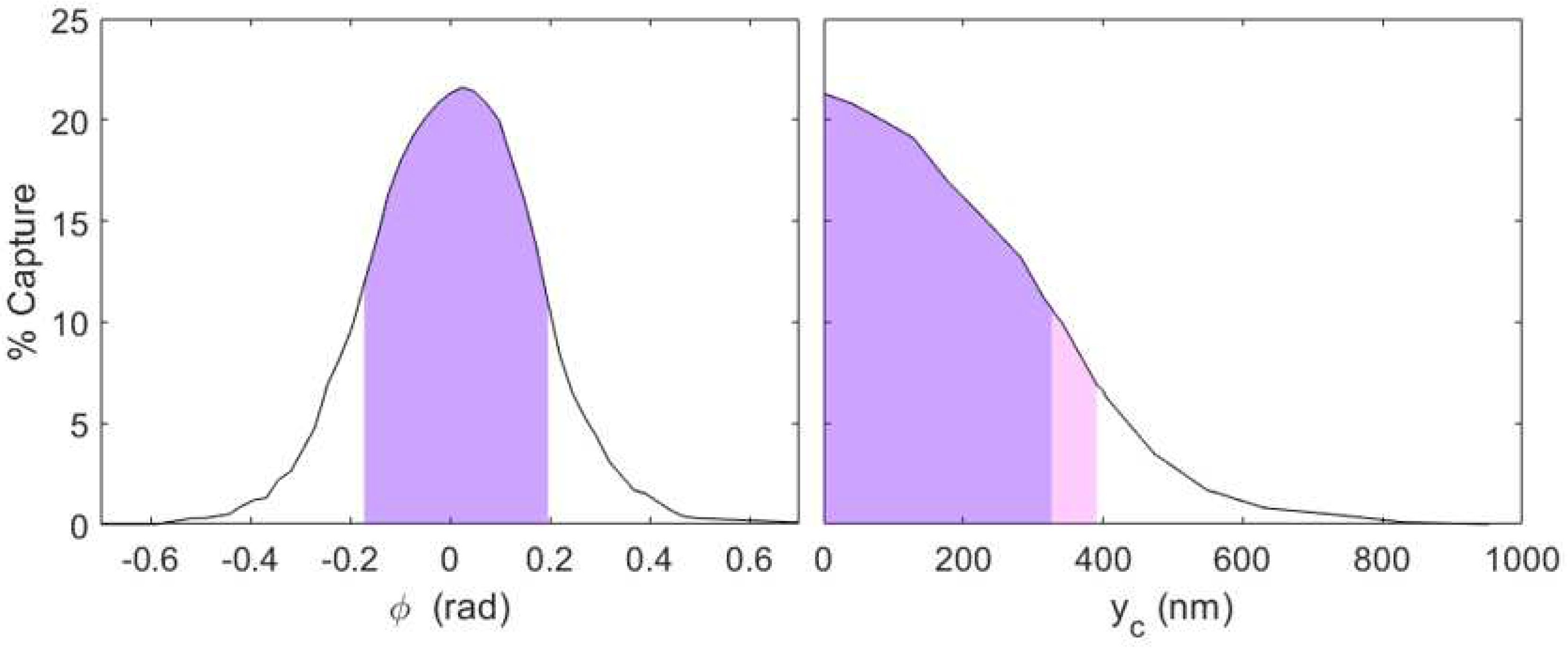
Figure 4.
The structure factor fits for an 800 nm gap, 50 % duty cycle symmetric structure. In a), grating offset is scanned over for each tooth height to retrieve maximum and minimum for each potential structure, shaded in blue. The black lineout represents the offset = 0 case. There is a clear maximum in potential at 650 nm tooth height, highlighted by the dashed lined. In b, a symmetric 650 nm tooth height structure is scanned over tooth width. A maxima is found for a 425 nm tooth width, although the structure is seen to be less sensitive to width than height.
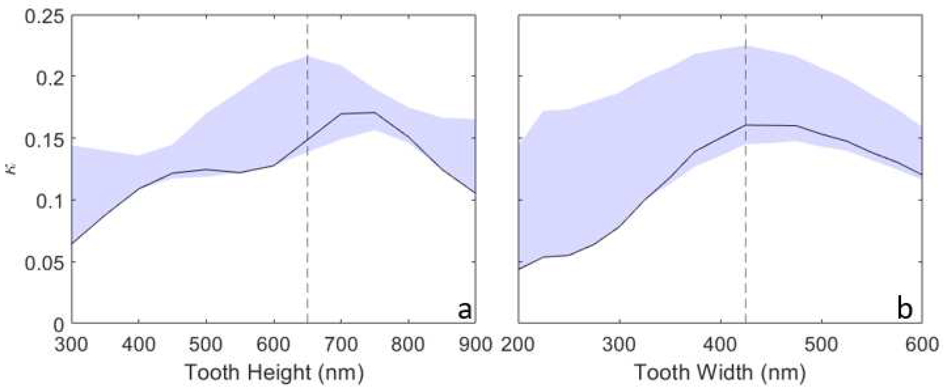
Figure 5.
The retrieved (left) and r (right) for an asymmetric structure with left tooth height of 450 nm and right tooth height of 650 nm. The tooth width for both gratings is 390 nm. For certain combinations of gap and offset may be set to 0; in this case, only gaps >= 800 nm have this capability. r generally decreases with increasing gap size, and has a similar periodic variation with offset as .
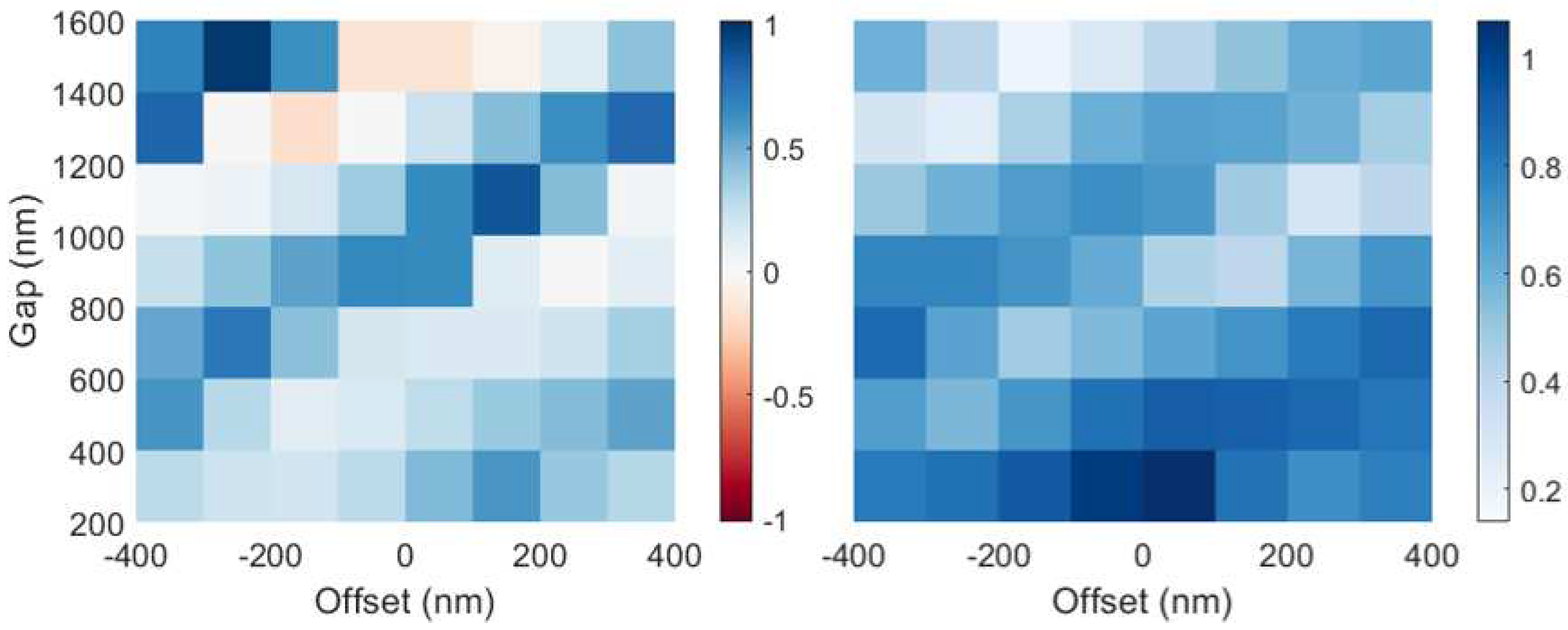
Figure 6.
Simulations scan over offset, gap, and left tooth height fit and parameters, from which and the effective gap are calculated. Each point corresponds to an offset which minimizes for that particular gap and tooth height combination; for all points above rad. Points are colored according to tooth width, shown on the colorbar and are sized by the absolute gap size, from 800 nm to 1600 nm in 200 nm steps. Higher tooth heights correspond to higher values. One can take the upper right boundary to be the Pareto front.
Disclaimer/Publisher’s Note: The statements, opinions and data contained in all publications are solely those of the individual author(s) and contributor(s) and not of MDPI and/or the editor(s). MDPI and/or the editor(s) disclaim responsibility for any injury to people or property resulting from any ideas, methods, instructions or products referred to in the content. |
© 2023 by the authors. Licensee MDPI, Basel, Switzerland. This article is an open access article distributed under the terms and conditions of the Creative Commons Attribution (CC BY) license (http://creativecommons.org/licenses/by/4.0/).
Copyright: This open access article is published under a Creative Commons CC BY 4.0 license, which permit the free download, distribution, and reuse, provided that the author and preprint are cited in any reuse.


